
\n\tWith the release of the 2nd generation iPad, Apple hopes to remain king of the tablet/slate PC market. The iPad 2 is thinner, lighter, and faster than the original Apple iPad. It also has front- and rear-facing cameras. Inside the iPad 2 are chips from Samsung, Texas Instruments, Broadcom, and more. Follow along as I crack open the Apple iPad 2 in this TR Dojo Teardown gallery.
\n\t
\n\tAnd if you’re thinking about buying on of the new iPads, check out Jason Hiner’s article, “Apple iPad 2: Who should buy and who should pass.”
\n\t
\n\tPhoto by: Bill Detwiler / TechRepublic
\n\tCaption by: Bill Detwiler
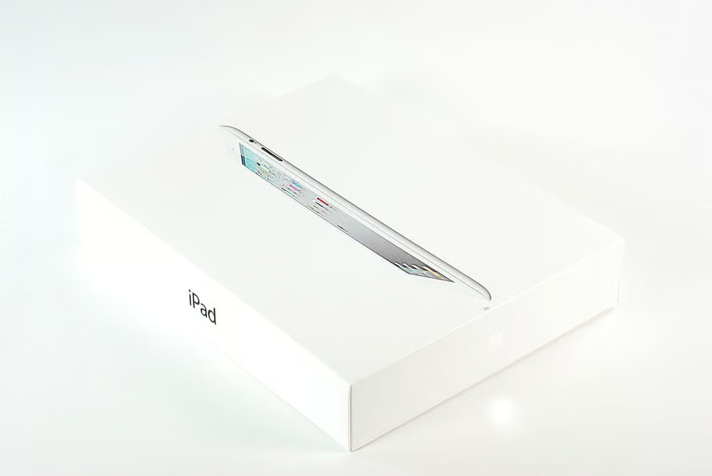
\n\tIn the US, the Apple iPad 2 is available in three storage sizes (16GB, 32GB, 64GB), two colors (black and white), and in three wireless configurations (Wi-Fi only, Wi-Fi + AT&T 3G, or Wi-Fi + Verizon 3G). We purchased this white, 16GB Wi-Fi only model at Target for $499 plus sales tax.
\n
\n\tFor a complete breakdown of prices by model, check out the Select your iPad page on Apple’s online store.
\n
\n\tPhoto by: Bill Detwiler / TechRepublic
\n\tCaption by: Bill Detwiler
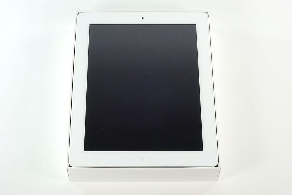
\n\tThe iPad 2has the following technical specifications:
\n
\n\t
\n\t
\n\t
\n\t
\n\t
\n
\n
\n\tPhoto by: Bill Detwiler / TechRepublic
\n\tCaption by: Bill Detwiler
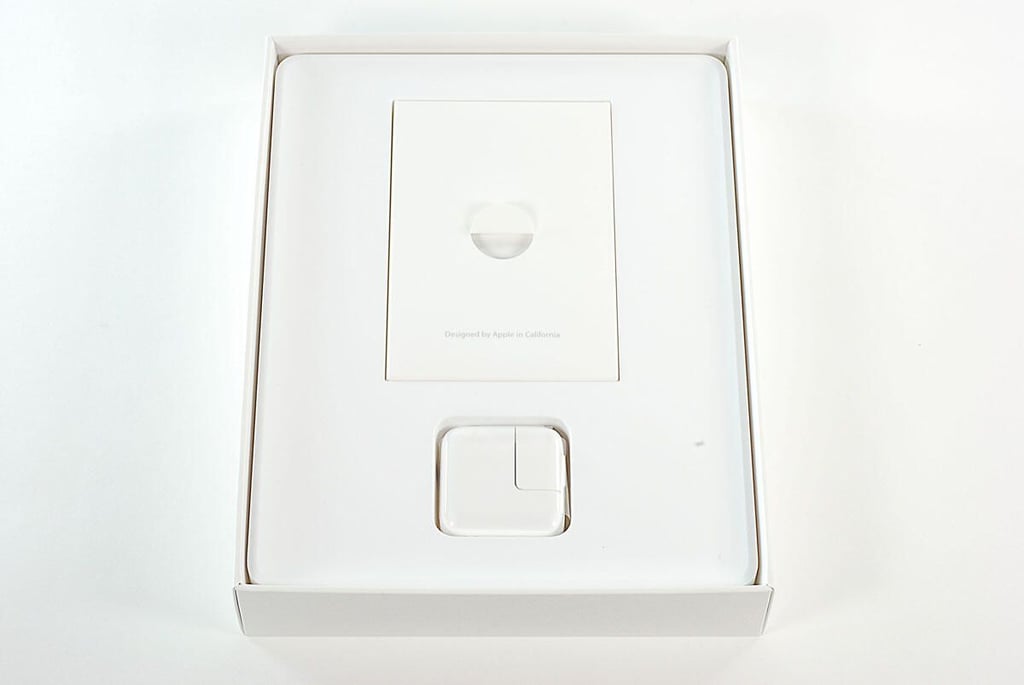
\n\tUnder the iPad 2 are the dock connector to USB cable, 10W USB power adapter, and product documentation.
\n
\n\tPhoto by: Bill Detwiler / TechRepublic
\n\tCaption by: Bill Detwiler
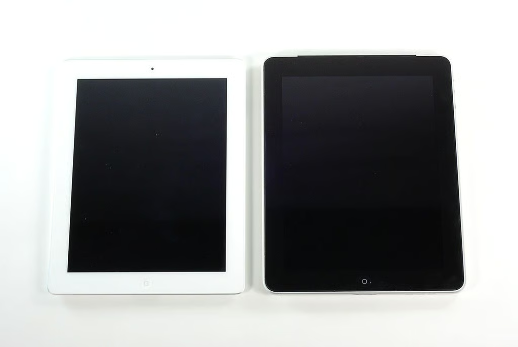
\n\tHere’s the iPad 2 (left) next to the original iPad 3G (right). The Apple iPad 2 weighs 1.35 lbs. (compared to the original iPad 3G’s 1.6 lbs.) and measures 9.5 x 7.31 x 0.34 inches (compared to the original iPad’s 9.56 x 7.47 x 0.5 inches).
\n
\n\tPhoto by: Bill Detwiler / TechRepublic
\n\tCaption by: Bill Detwiler
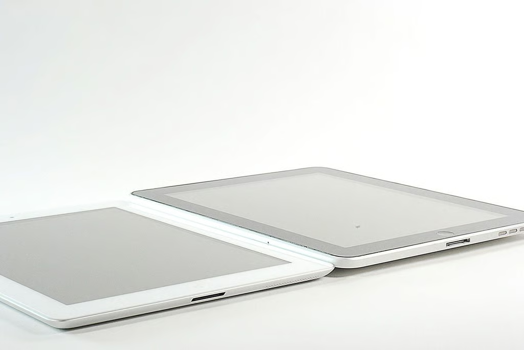
\n\tLooking at both the iPad 2 (left) and iPad 3G (right) from this angle, you can see the significant difference in height between the two tablets. The newer tablet also has a beveled edge, which makes the iPad 2 feel even thinner than it actually is.
\n
\n\tPhoto by: Bill Detwiler / TechRepublic
\n\tCaption by: Bill Detwiler
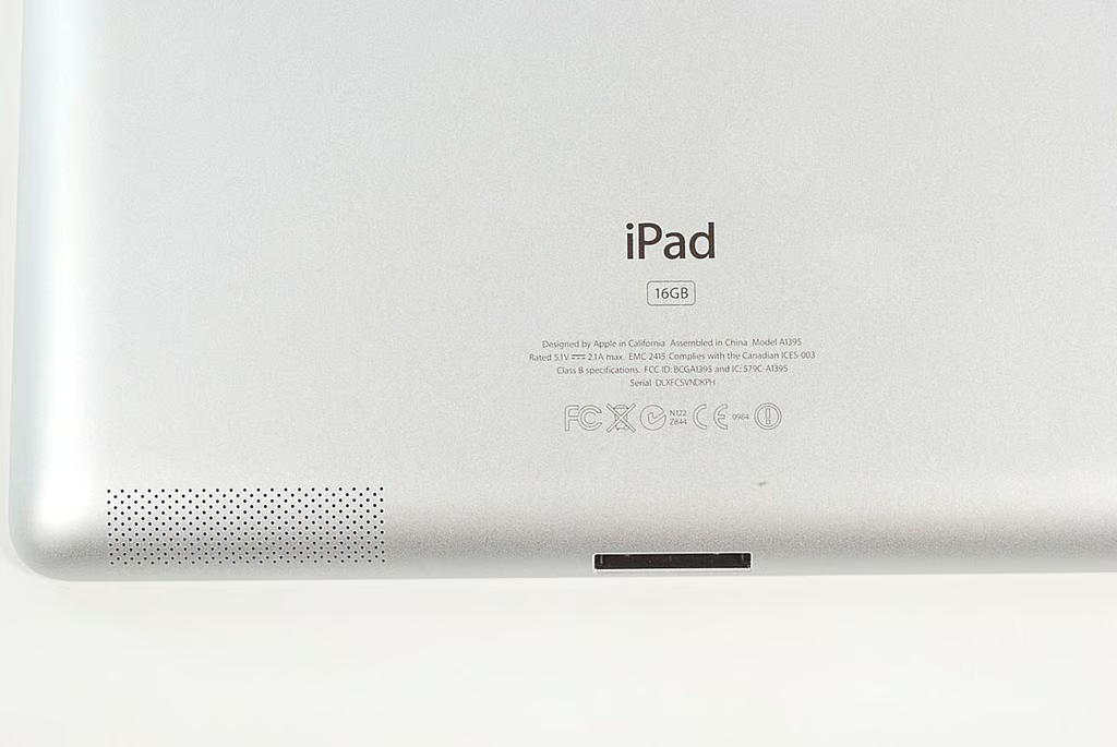
\n\tAlong the bottom of the iPad 2 are the 30-pin dock connector and speaker grill. The iPad 2’s model number is A1395.
\n
\n\tPhoto by: Bill Detwiler / TechRepublic
\n\tCaption by: Bill Detwiler
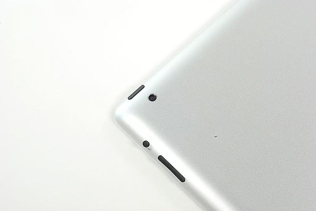
\n\tAlong the top edge of the iPad 2 are the On/off and Sleep/wake button, rear-facing camera, Silent/Screen rotation lock button, and volume up/down button. The 3.5mm headphone jack is also located along the top edge.
\n
\n\tPhoto by: Bill Detwiler / TechRepublic
\n\tCaption by: Bill Detwiler
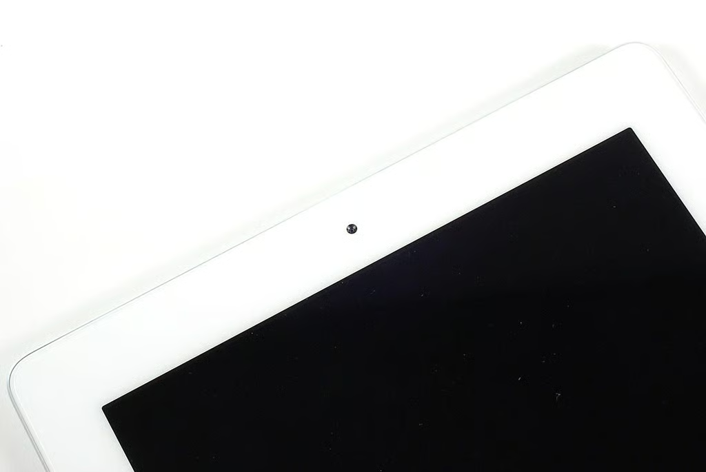
\n\tThe Apple iPad 2’s front-facing camera and ambient light sensor are located along the top of the front panel.
\n
\n\tPhoto by: Bill Detwiler / TechRepublic
\n\tCaption by: Bill Detwiler
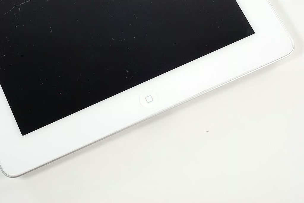
\n\tThe iPad 2’s Home button is located at the bottom of the front panel in the center.
\n
\n\tPhoto by: Bill Detwiler / TechRepublic
\n\tCaption by: Bill Detwiler
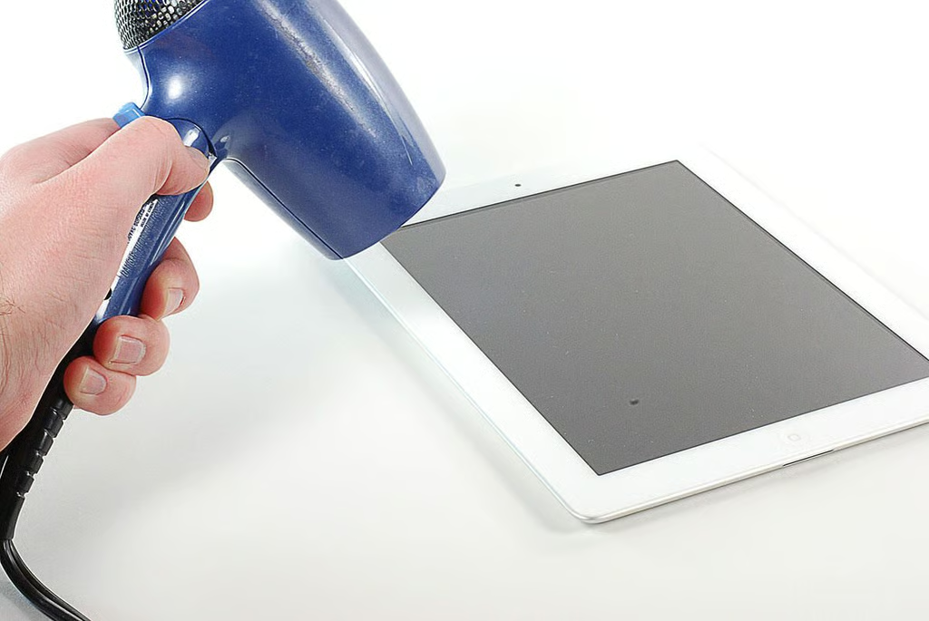
\n\tApple used metal clips to hold the original iPad and iPad 3G’s front panel in place. On the iPad 2, Apple abbandoned the clips for extermely strong adhesive. To remove the front glass panel, I first heated the edges with a hair dryer.
\n
\n\tPhoto by: Bill Detwiler / TechRepublic
\n\tCaption by: Bill Detwiler
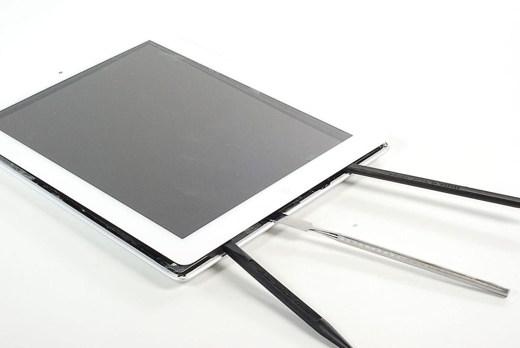
\n\tWhile heating the edges of the iPad 2’s front panel, I used several plastic and metal tools to gently pry the panel away from the frame. This was by far the longest part of the teardown. It took at least an hour to remove the front panel. I was able to remove the panel without cracking the glass, but it was a very slow process.
\n
\n\tPhoto by: Bill Detwiler / TechRepublic
\n\tCaption by: Bill Detwiler
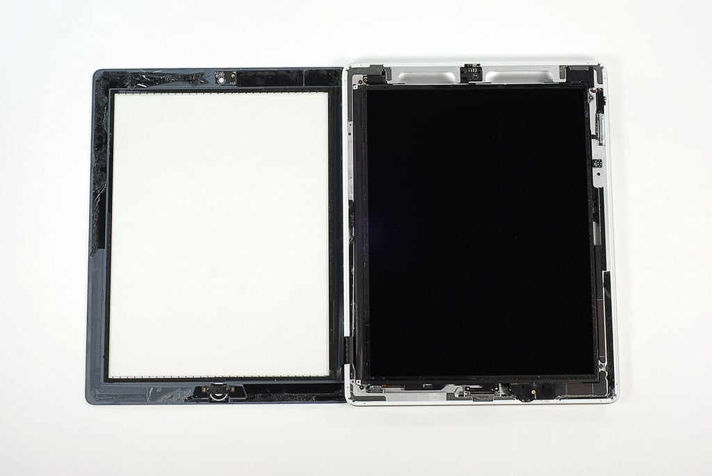
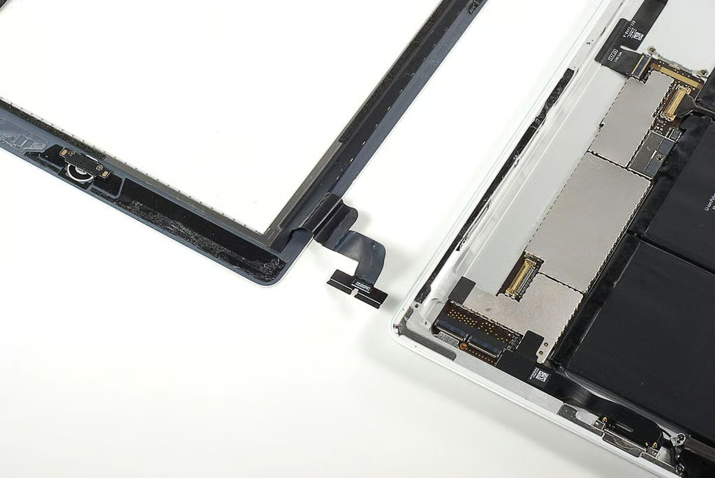
\n\tThe front panel is connected to the rest of the iPad 2 with a thin ribbon cable. I’ll need to disconnect the ribbon cable before separating the two halves of the iPad 2.
\n
\n\tPhoto by: Bill Detwiler / TechRepublic
\n\tCaption by: Bill Detwiler
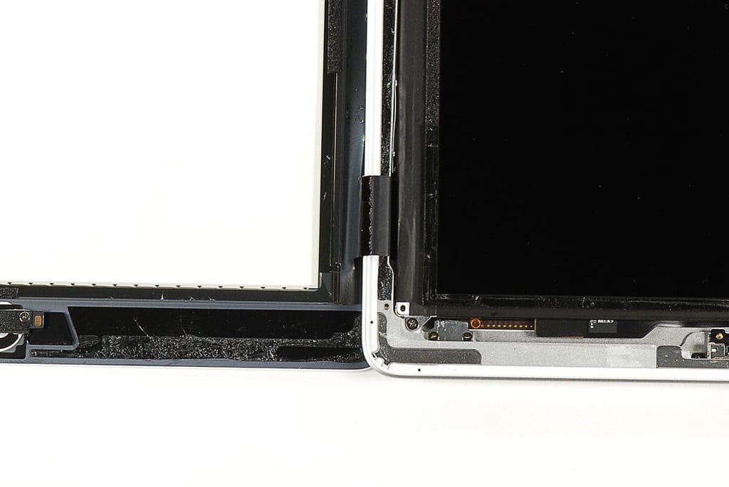
\n\tThis photo shows the ribbon cable that connects the front panel’s digitizer to the iPad 2’s main system board.
\n
\n\tPhoto by: Bill Detwiler / TechRepublic
\n\tCaption by: Bill Detwiler
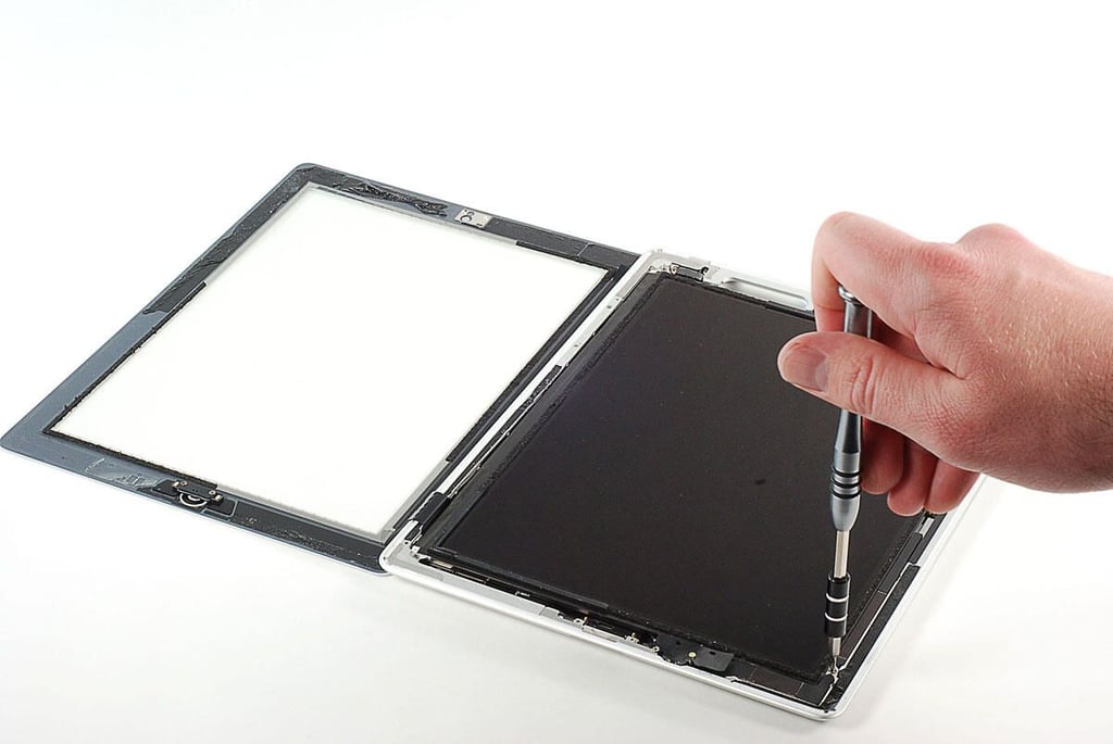
\n\tBefore disconnecting the front panel’s ribbon cable, I’ll need to remove the LCD, which covers the connector and most of the iPad 2’s internal components. Luckily, Apple uses standard Phillps #00 screws inside the iPad 2’s case.
\n
\n\tPhoto by: Bill Detwiler / TechRepublic
\n\tCaption by: Bill Detwiler
\n\tAfter removing the four Phillips #00 screws that hold the iPad 2’s LCD in place, I was able to lift it up from the frame.
\n
\n\tPhoto by: Bill Detwiler / TechRepublic
\n\tCaption by: Bill Detwiler
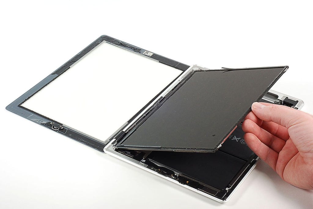
\n\tThe LCD is connected to the iPad 2’s main PCB with a single cable. I’ll need to disconnect the cable before completely removing the LCD.
\n
\n\tPhoto by: Bill Detwiler / TechRepublic
\n\tCaption by: Bill Detwiler
\n\tThe LCD’s ribbon cable connector has a small handle that you can hold when detaching the cable from the iPad 2’s main PCB.
\n
\n\tPhoto by: Bill Detwiler / TechRepublic
\n\tCaption by: Bill Detwiler
\n\tWith the LCD cable detached, you can completely remove the Apple iPad 2’s LCD from the frame.
\n
\n\tPhoto by: Bill Detwiler / TechRepublic
\n\tCaption by: Bill Detwiler
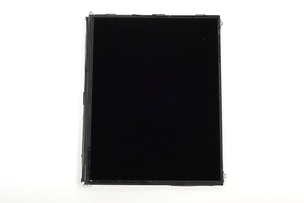
\n\tThe Apple iPad 2’s 9.7-inch (diagonal) LED-backlit LCD delivers a 1024×768 resolution at 132 pixels per inch.
\n
\n\tPhoto by: Bill Detwiler / TechRepublic
\n\tCaption by: Bill Detwiler
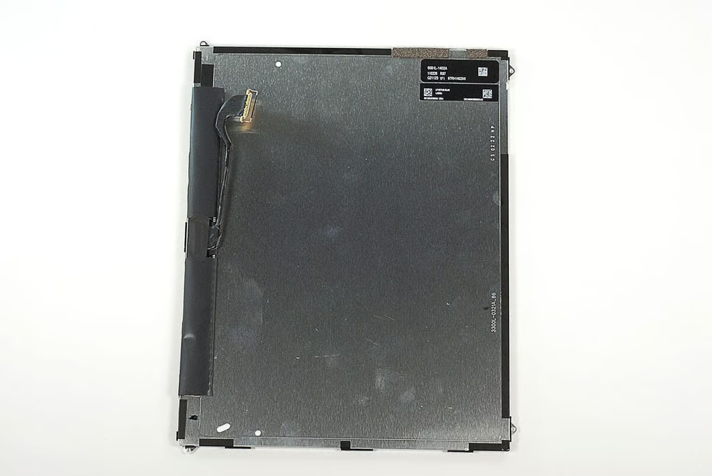
\n\tPhoto by: Bill Detwiler / TechRepublic
\n\tCaption by: Bill Detwiler
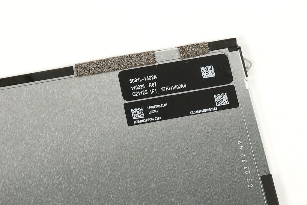
\n\tThe labels on the back of the Apple iPad 2’s LCD have the following markings:
\n
\n\t6091L-1402A
\n\t110226 R87
\n\tQ2112S 1F1 87RH1402A6
\n
\n\tLP 097X02-SLN1
\n\tLGDNJ
\n\t097A2N4303HX4 322A
\n\tC8CA99650B9DD31A3
\n
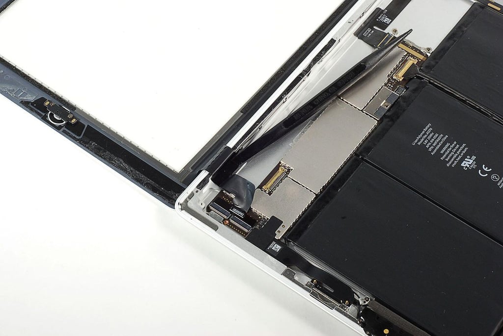
\n\tPhoto by: Bill Detwiler / TechRepublic
\n\tCaption by: Bill Detwiler
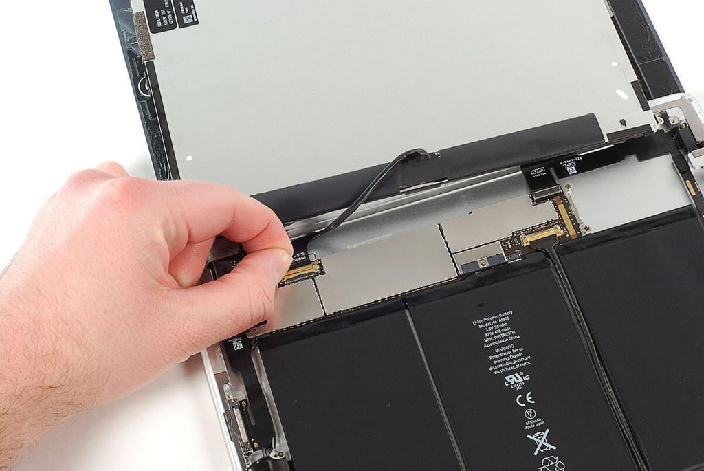
\n\tThe ribbon cable for the front panel’s digitizer is attached to the Apple iPad 2’s main PCB via two connectors. The cable is also attached to one of the metal EMI shields on the main PCB with adhesive. I was able to gently peel the cable away from the shield. And after lifting the catch on both connectors, I detached the cable.
\n
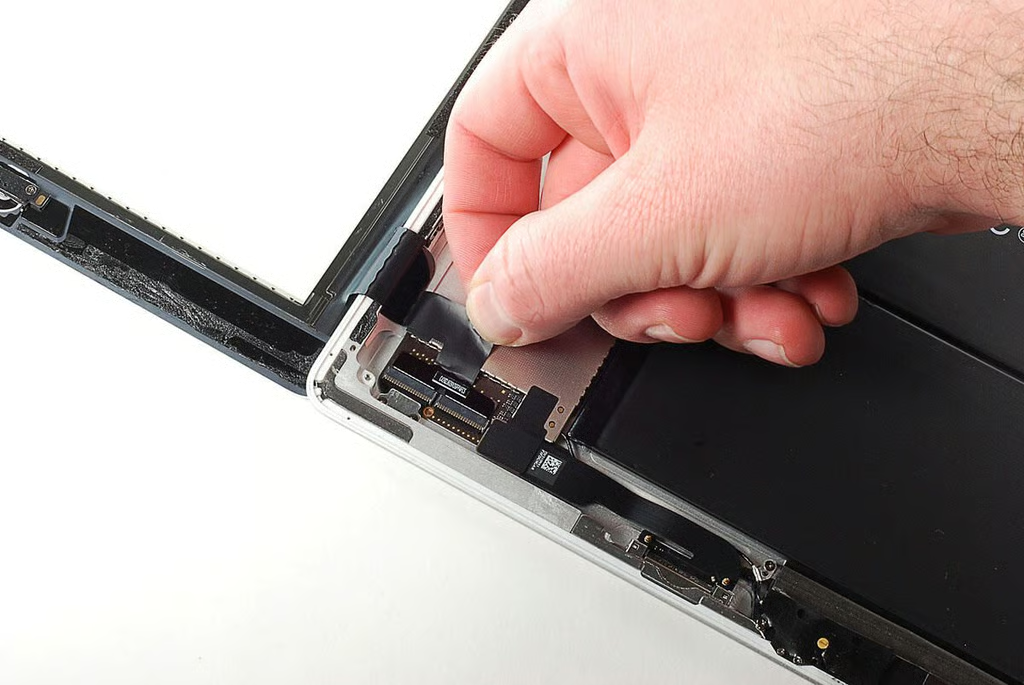
\n\tPhoto by: Bill Detwiler / TechRepublic
\n\tCaption by: Bill Detwiler
\n\tThe front panel’s cable is also attached to the Apple iPad 2’s frame with adhesive. Using a plastic spudger, I was able to detach the cable from the frame.
\n
\n\tPhoto by: Bill Detwiler / TechRepublic
\n\tCaption by: Bill Detwiler
\n\tPhoto by: Bill Detwiler / TechRepublic
\n\tCaption by: Bill Detwiler
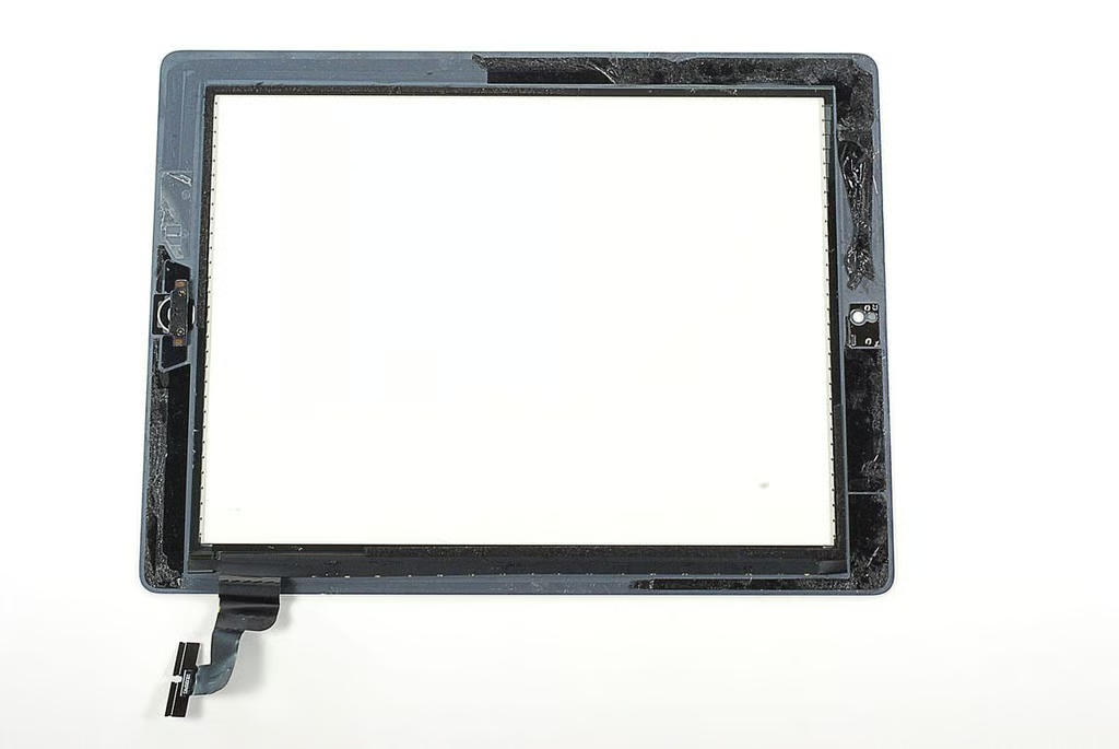
\n\tThe iPad 2’s front panel is significantly thinner than the one used on the original iPad. I also seems to be more flexible. According to Apple’s website, the glass has a “fingerprint-resistant oleophobic coating”. I’m not sure about resisting finger prints, but when placed front-side down the panel slid all over the table in our photo studio.
\n
\n\tPhoto by: Bill Detwiler / TechRepublic
\n\tCaption by: Bill Detwiler
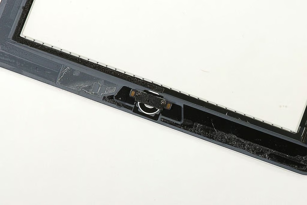
\n\tThe Home button is attached to the Apple iPad 2’s front panel two Phillips #00 screws and a small bracket.
\n
\n\tPhoto by: Bill Detwiler / TechRepublic
\n\tCaption by: Bill Detwiler
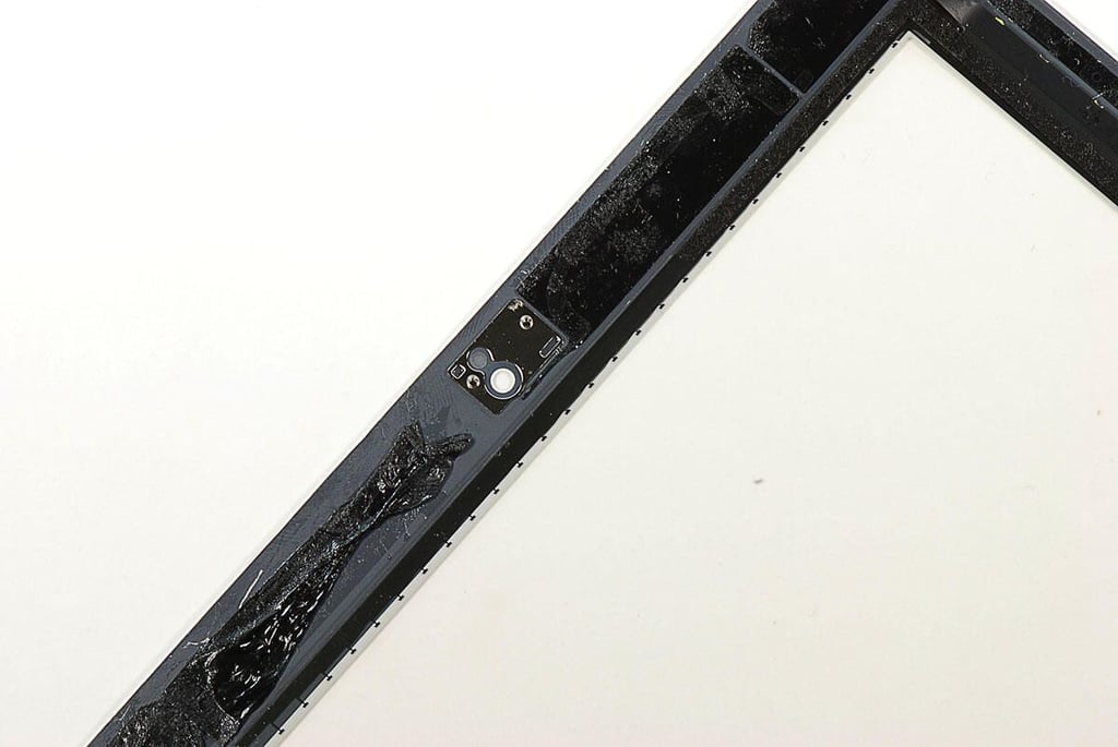
\n\tThese two clear spots are for the Apple iPad 2’s front-facing camera and ambient light sensor.
\n
\n\tPhoto by: Bill Detwiler / TechRepublic
\n\tCaption by: Bill Detwiler
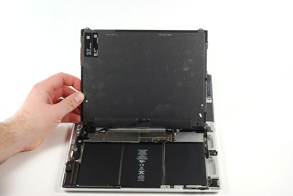
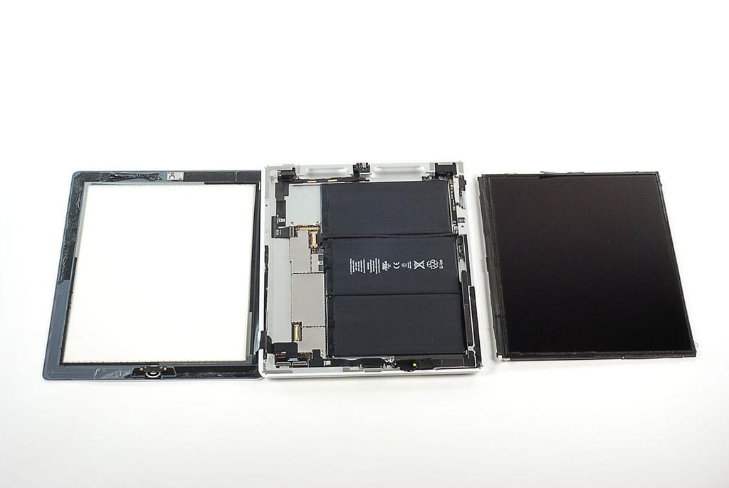
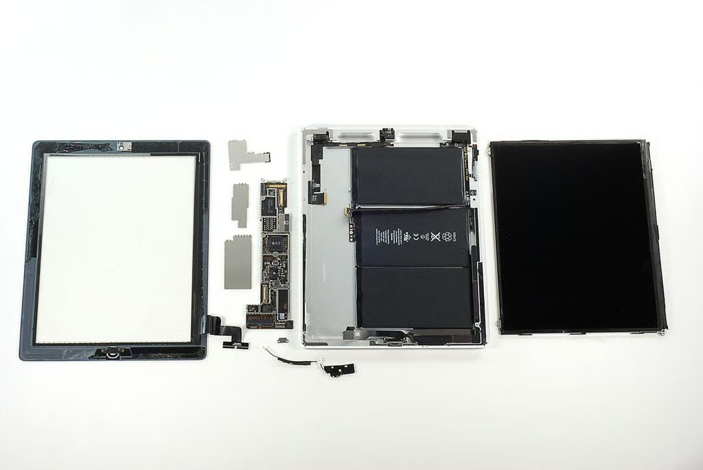
\n\tWith the LCD and front panel completely removed, we get our first unobstructed view inside the Apple iPad 2.
\n
\n\tPhoto by: Bill Detwiler / TechRepublic
\n\tCaption by: Bill Detwiler
\n\tBefore removing the Apple iPad 2’s main PCB, I’m going to remove the Wi-Fi antenna, which is attached to the frame with two Phillips #00 screws.
\n
\n\tPhoto by: Bill Detwiler / TechRepublic
\n\tCaption by: Bill Detwiler
\n\tThe Apple iPad 2’s Wi-Fi antenna wire run under the ribbon cable for the Home button. Unfortunately, this ribbon cable is also glued to one of the EMI shields on the main PCB and the frame. Using a thin metal blade, I peeled the Home button’s ribbon cable away from the EMI shield.
\n
\n\tPhoto by: Bill Detwiler / TechRepublic
\n\tCaption by: Bill Detwiler
\n\tAfter peeling the Home button ribbon cable away from the EMI shield, I popped loose its connector from the Apple iPad 2’s main PCB.
\n
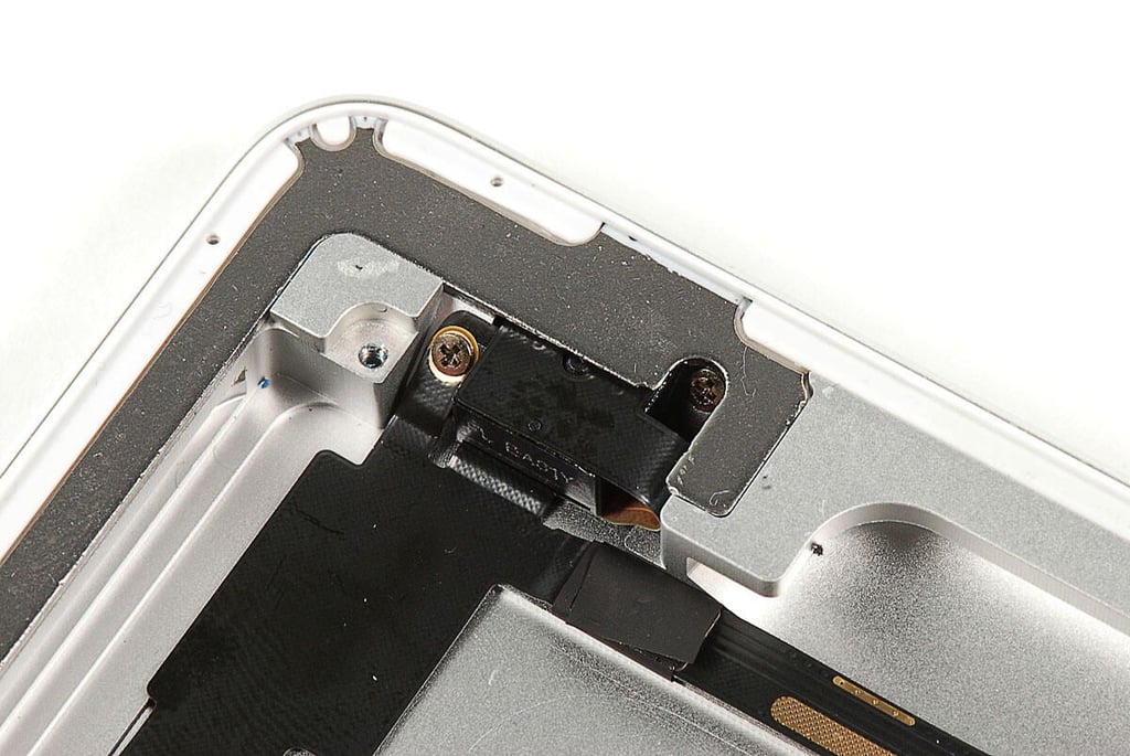
\n\tPhoto by: Bill Detwiler / TechRepublic
\n\tCaption by: Bill Detwiler
\n\tUnder the Home button’s ribbon cable, there’s also a connector for a wire that goes to the Apple iPad 2’s speaker.
\n
\n\tPhoto by: Bill Detwiler / TechRepublic
\n\tCaption by: Bill Detwiler
\n\tThe Home button ribbon cable, speaker wire, and Wi-Fi antenna wire are all glued to the Apple iPad 2’s frame. I was able to gently peel them all loose.
\n
\n\tPhoto by: Bill Detwiler / TechRepublic
\n\tCaption by: Bill Detwiler
\n\tFinally, the Wi-Fi antenna comes free from the Apple iPad 2’s frame.
\n
\n\tPhoto by: Bill Detwiler / TechRepublic
\n\tCaption by: Bill Detwiler
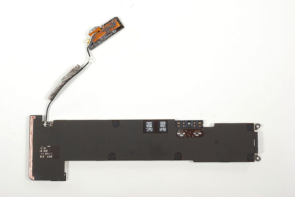
\n\tAfter disconnecting the lower cables and peeling free the Wi-Fi antenna wire, I turned my attention to the connector for the the Apple iPad 2’s rear-facing camera, volume up/down button, on/off sleep/wake button, and silent/screen rotation lock switch. Like the LCD connector, this one has a handle with which you can pull it loose from the main PCB.
\n
\n\tPhoto by: Bill Detwiler / TechRepublic
\n\tCaption by: Bill Detwiler
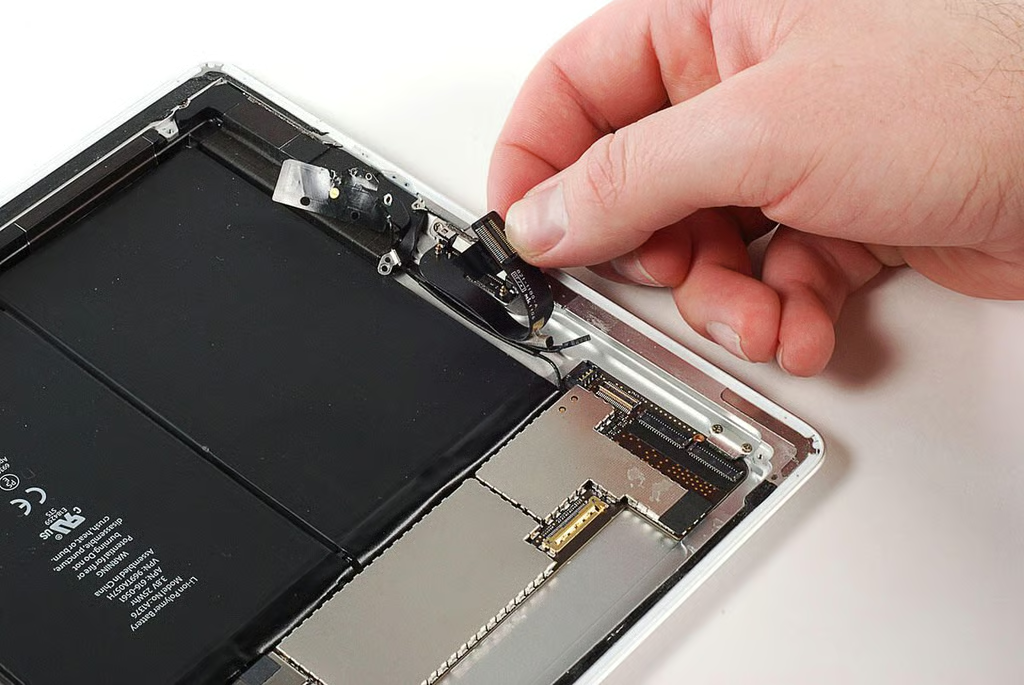
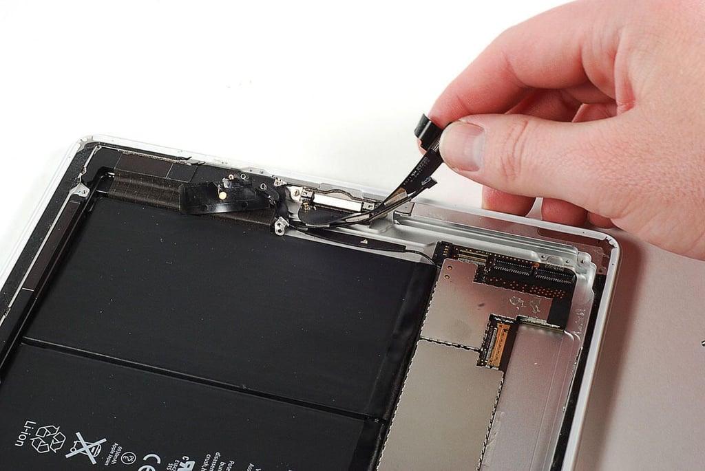
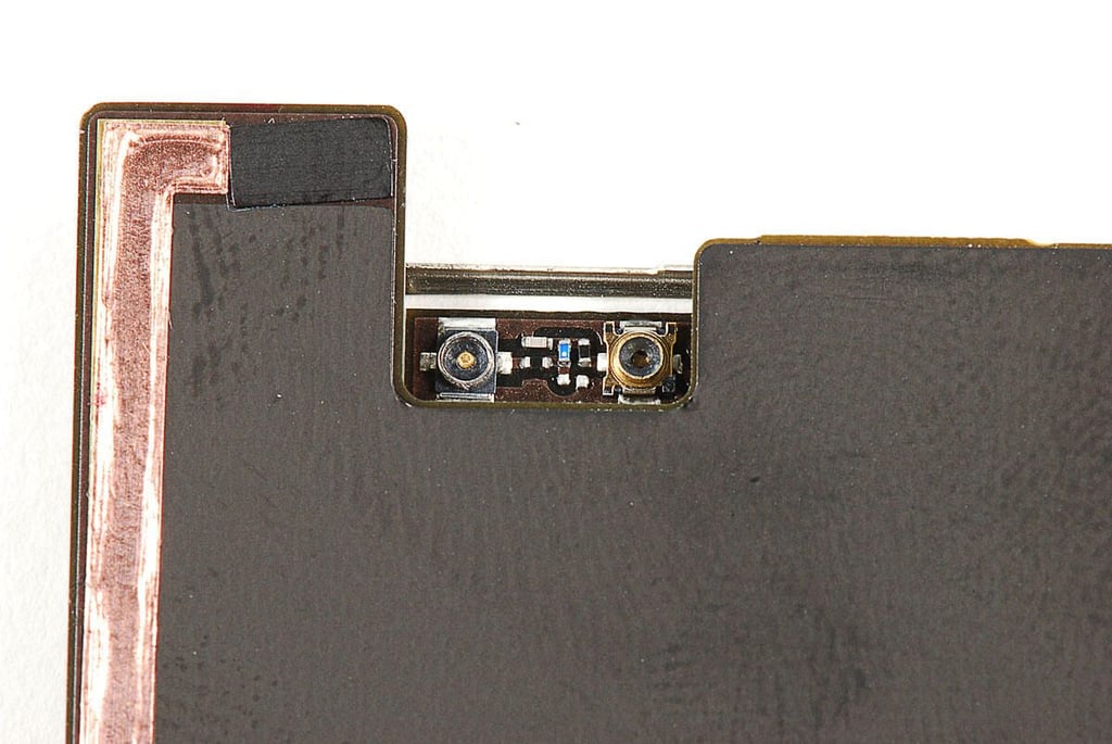
\n\tWith the cable for the rear-facing camera and nearby buttons disconnected, I’ll next disconnect the cable for the Apple iPad 2’s front-facing camera.
\n
\n\tPhoto by: Bill Detwiler / TechRepublic
\n\tCaption by: Bill Detwiler
\n\tThe ribbon cable for the Apple iPad 2’s front-facing camera is glued to the frame and attached to the main PCB with a gated connected. I lifted the catch up, but did pull the cable out of the connector. I’ll let is slip out when I remove the main PCB from the frame.
\n
\n\tPhoto by: Bill Detwiler / TechRepublic
\n\tCaption by: Bill Detwiler
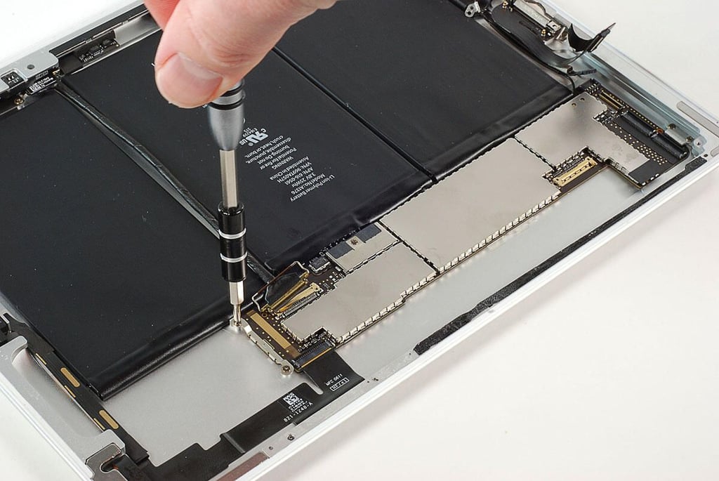
\n\tWith all the cable disconnected, I removed the four Phillips #00 screws that hold the Apple iPad’s main PCB to the frame.
\n
\n\tPhoto by: Bill Detwiler / TechRepublic
\n\tCaption by: Bill Detwiler
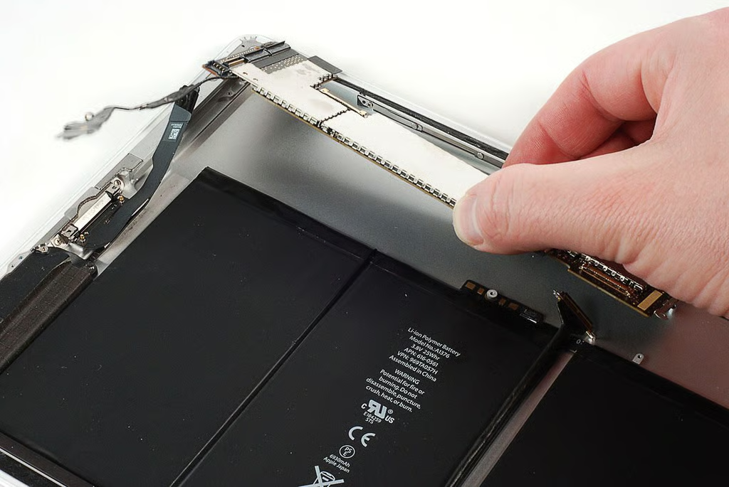
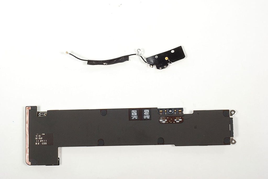
\n\tWith the screws removed and all the cable disconnected, I lifted the Apple iPad 2’s main PCB away from the metal frame. The Wi-Fi antenna is still connected to the board.
\n
\n\tPhoto by: Bill Detwiler / TechRepublic
\n\tCaption by: Bill Detwiler
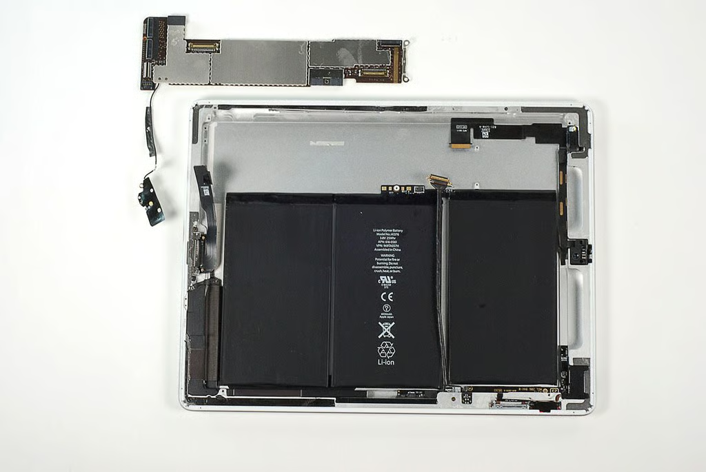
\n\tI left the Wi-Fi antenna connected to the Apple iPad 2’s main PCB.
\n
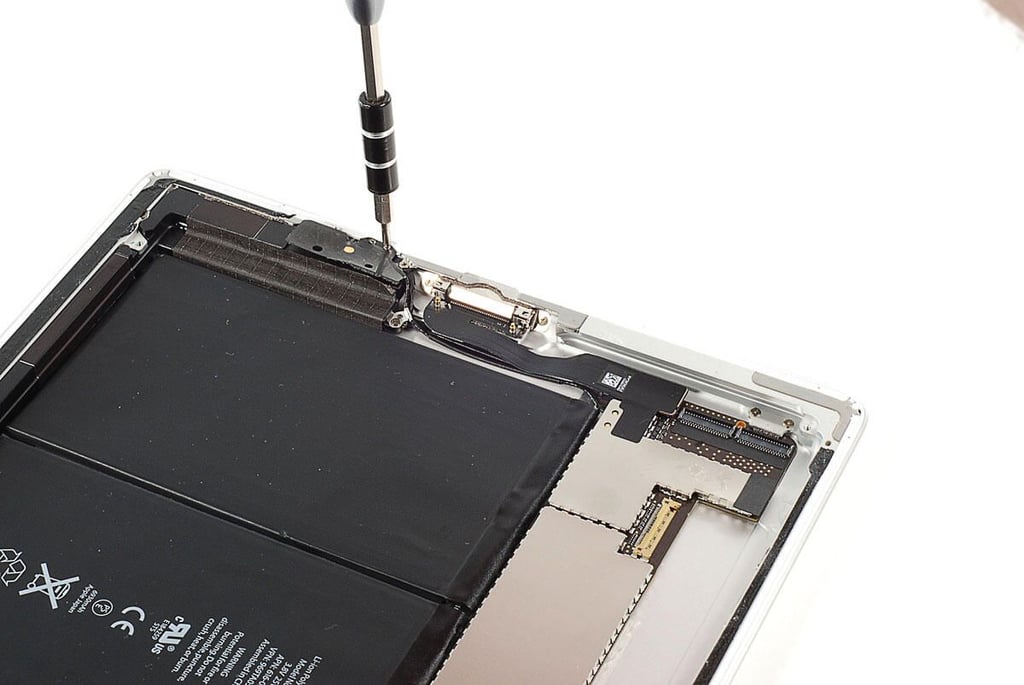
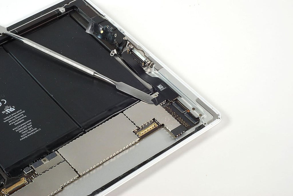
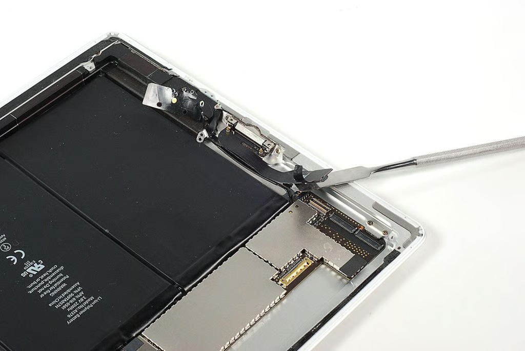
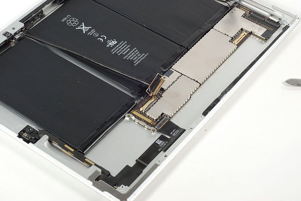
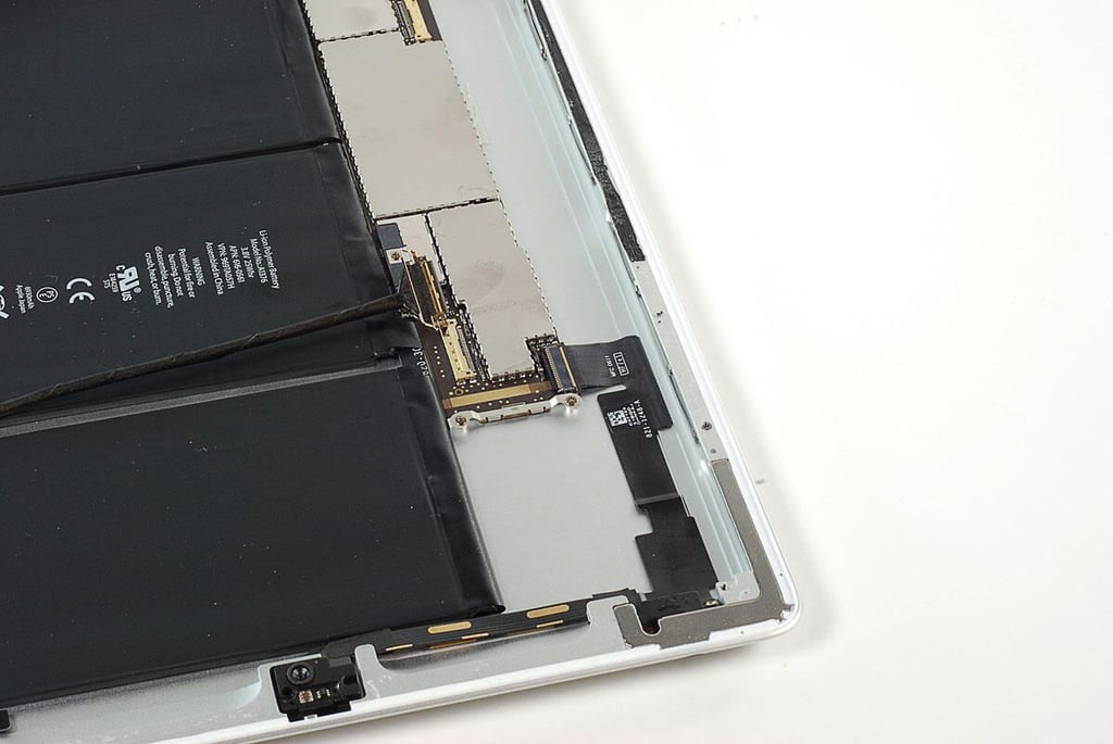
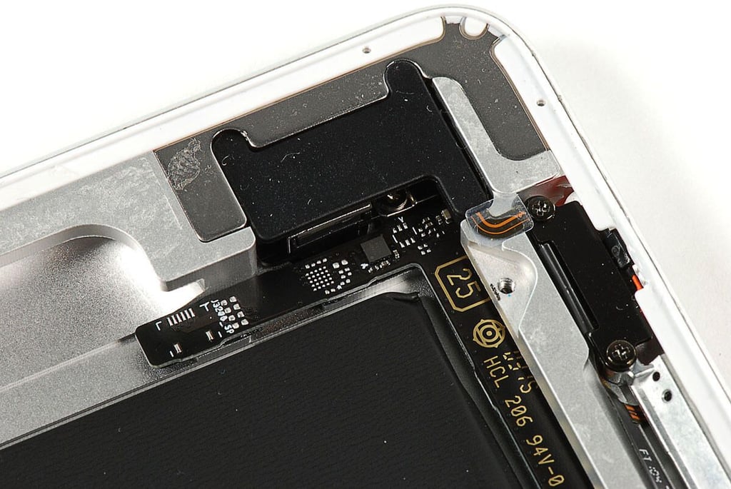
\n\tPhoto by: Bill Detwiler / TechRepublic
\n\tCaption by: Bill Detwiler
\n\tBefore turning our attention to the main PCB, let’s look at the components still attached to the Apple iPad 2’s metal frame.
\n
\n\tAfter careful consideration, I decided to leave them in place. I want to reassemble this iPad 2 in working order. As nearly all the remaining components or their ribbon cables are glued to the frame, I feared removing them might cause damage.
\n
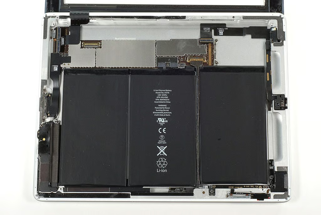
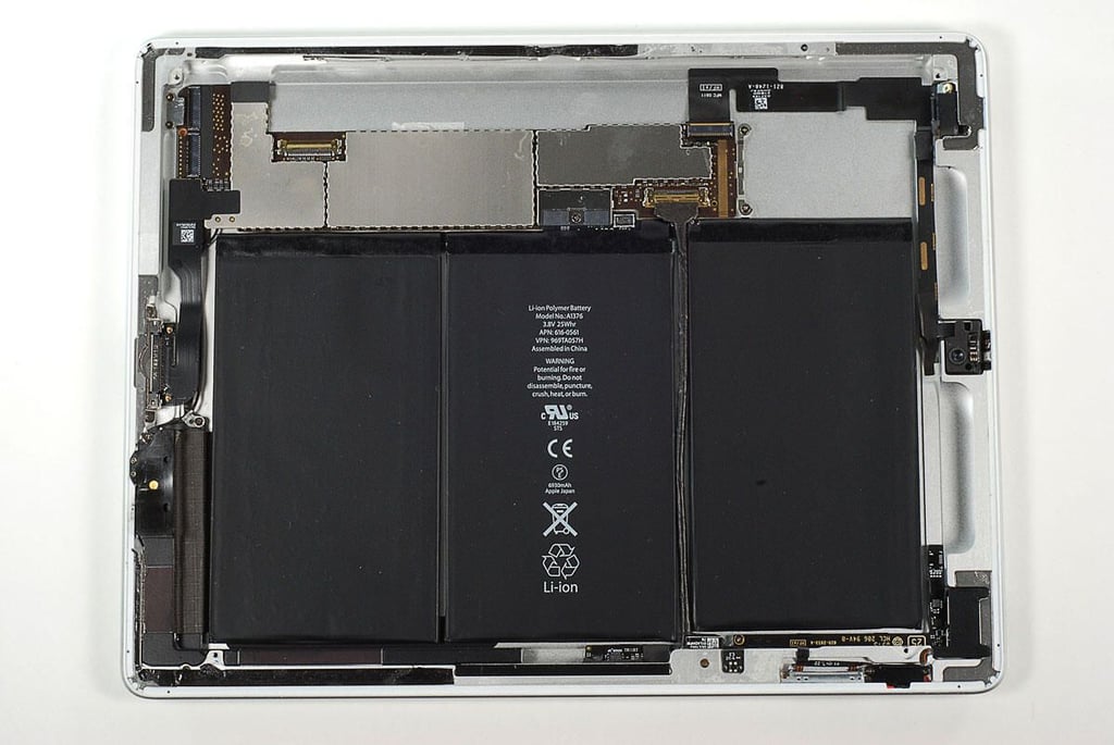
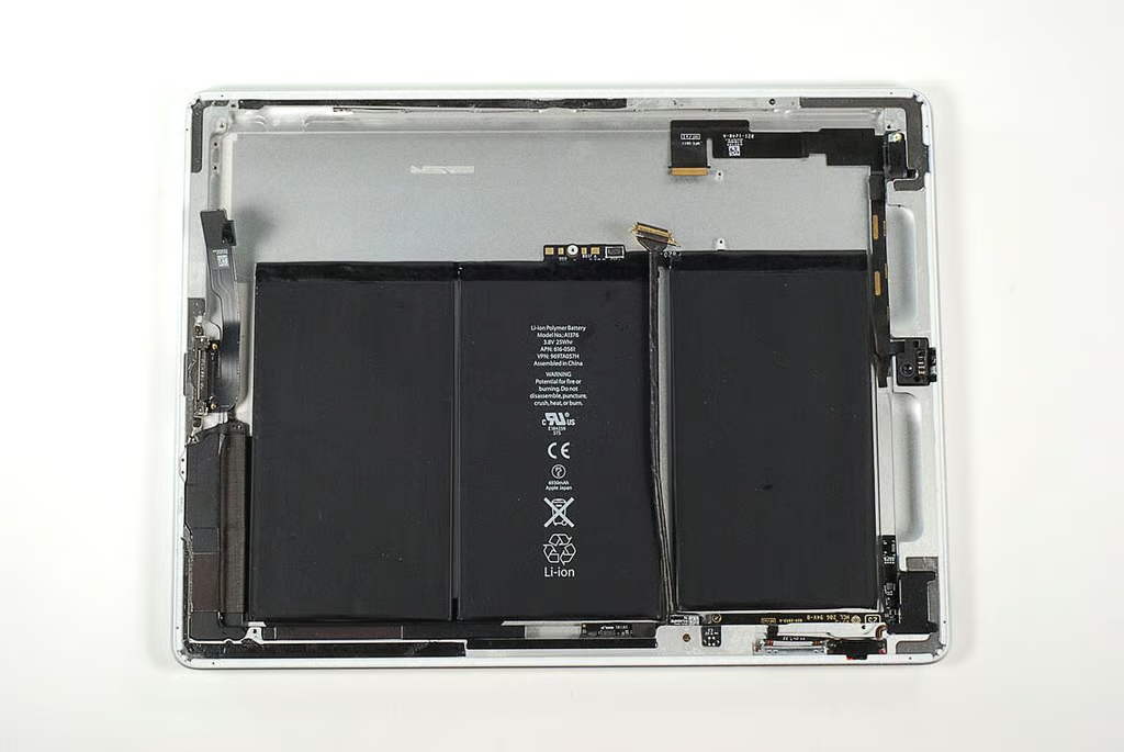
\n\tPhoto by: Bill Detwiler / TechRepublic
\n\tCaption by: Bill Detwiler
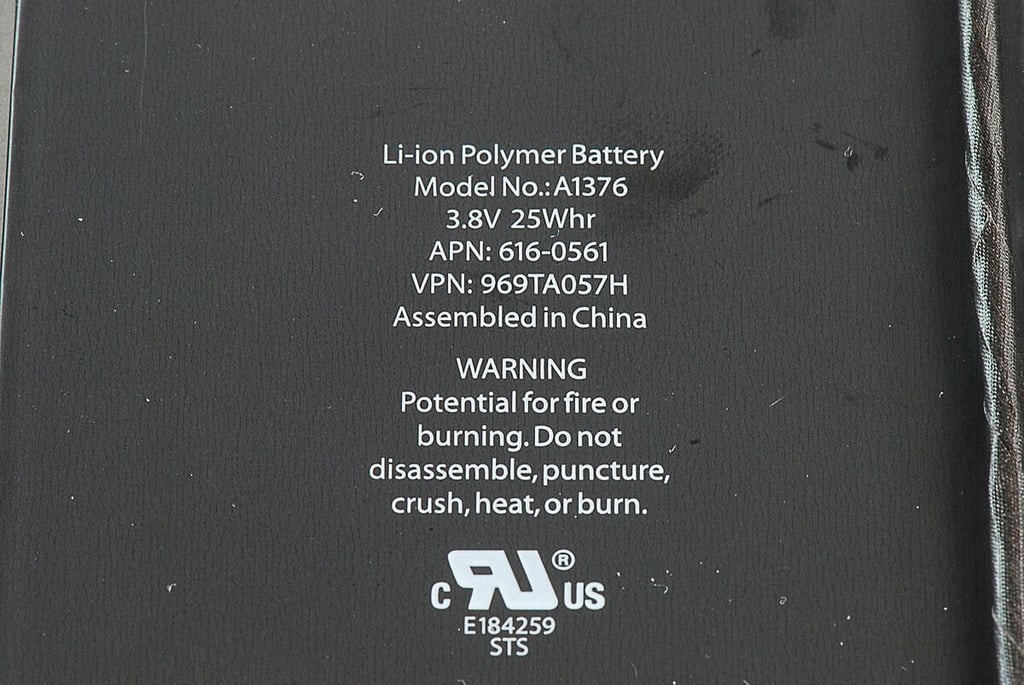
\n\tThe Apple iPad 2 has a 3.8V 25 Whr Li-Ion Polymer battery.
\n
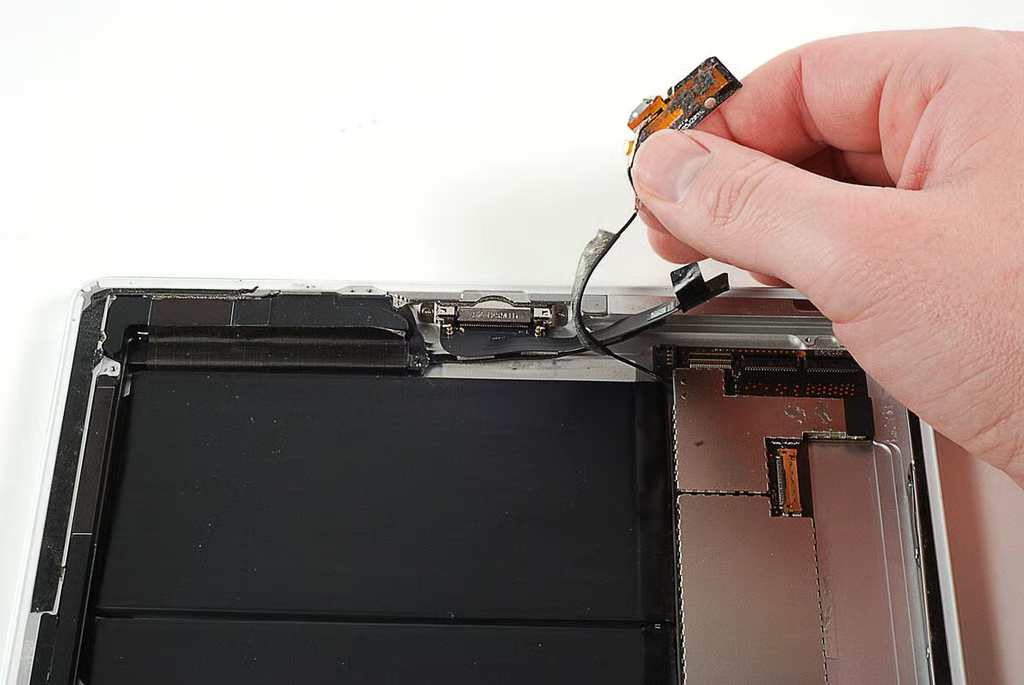
\n\tPhoto by: Bill Detwiler / TechRepublic
\n\tCaption by: Bill Detwiler
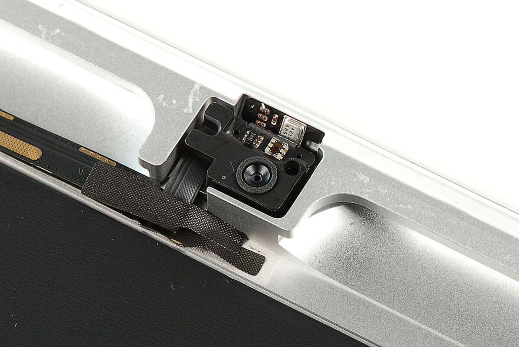
\n\tThe Apple iPad 2’s front-facing camera can record VGA video at up to 30 fps and shoot VGA-quality stills. Above the camera is the ambient light sensor.
\n
\n\tPhoto by: Bill Detwiler / TechRepublic
\n\tCaption by: Bill Detwiler
\n\tIn the Apple iPad 2’s upper-left corner is the 3.5mm stereo headphone jack.
\n
\n\tPhoto by: Bill Detwiler / TechRepublic
\n\tCaption by: Bill Detwiler
\n\tIn the Apple iPad 2’s upper-right corner, are the power on/off sleep/wake button, and silent screen rotation lock switch, and rear-facing camera.
\n
\n\tPhoto by: Bill Detwiler / TechRepublic
\n\tCaption by: Bill Detwiler
\n\tJust below the silent/screen rotation lock switch is the Apple iPad 2’s volume up/down button.
\n
\n\tPhoto by: Bill Detwiler / TechRepublic
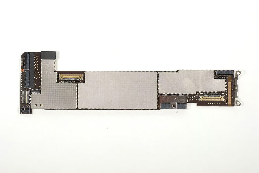
\n\tCaption by: Bill Detwiler
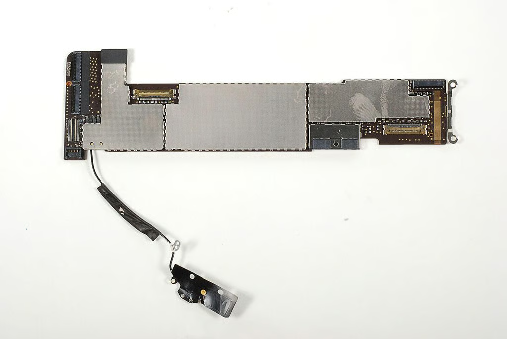
\n\tThe Apple iPad 2’s main PCB is significantly longer than the main board on the original iPad 3G.
\n
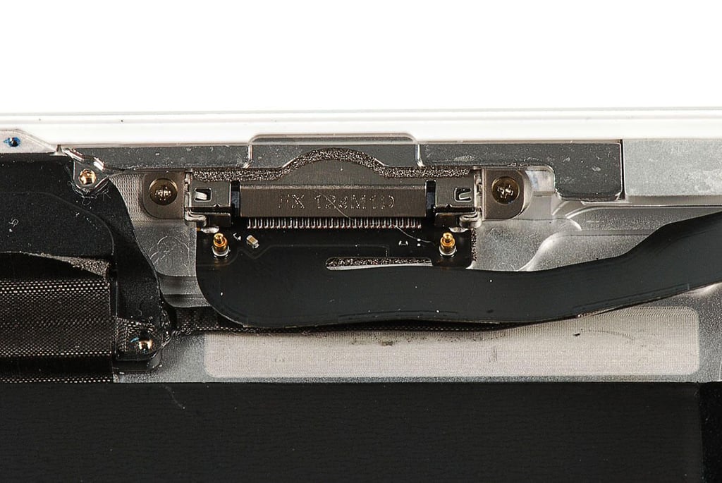
\n\tPhoto by: Bill Detwiler / TechRepublic
\n\tCaption by: Bill Detwiler
\n\tThe connector for the Apple iPad 2’s Wi-Fi antenna is access through the underside of the main PCB.
\n
\n\tPhoto by: Bill Detwiler / TechRepublic
\n\tCaption by: Bill Detwiler
\n\tI detached the Apple iPad 2’s Wi-Fi antenna wire from the main PCB with thin metal blade.
\n
\n\tPhoto by: Bill Detwiler / TechRepublic
\n\tCaption by: Bill Detwiler
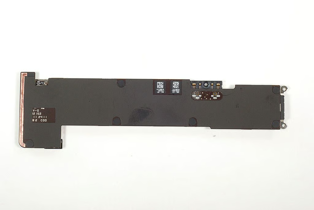
\n\tWith the Wi-Fi antenna removed, let’s take a closer look at the underside of the Apple iPad 2’s main PCB.
\n
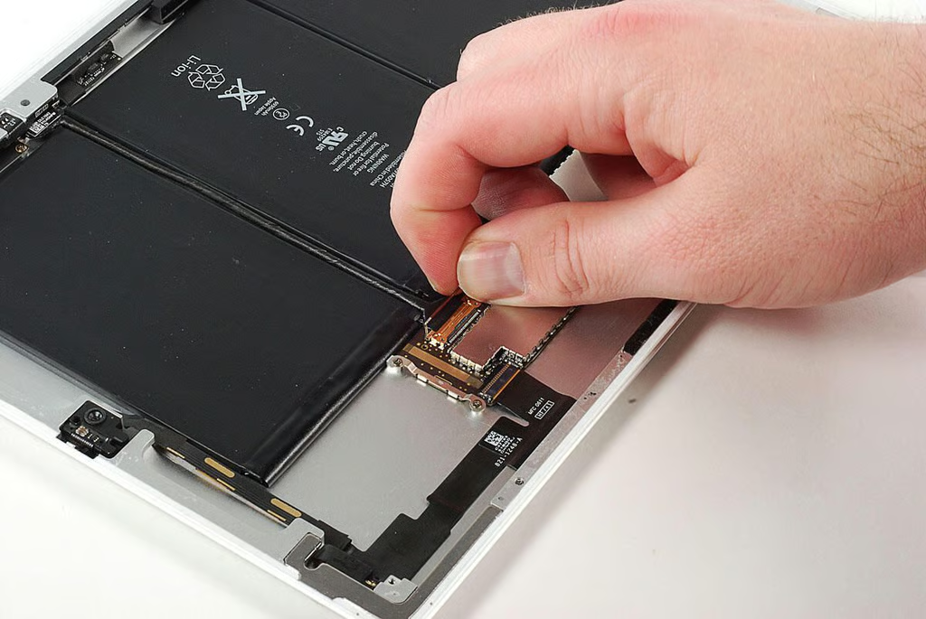
\n\tPhoto by: Bill Detwiler / TechRepublic
\n\tCaption by: Bill Detwiler
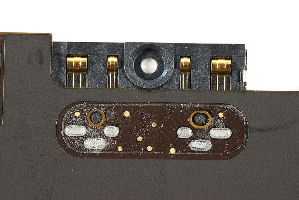
\n\tThe Apple iPad 2 battery connects to the main PCB via these contacts.
\n
\n\tPhoto by: Bill Detwiler / TechRepublic
\n\tCaption by: Bill Detwiler
\n\tThe Apple iPad 2’s wireless card has two contacts. Only one was being used for Wi-Fi antenna.
\n
\n\tPhoto by: Bill Detwiler / TechRepublic
\n\tCaption by: Bill Detwiler
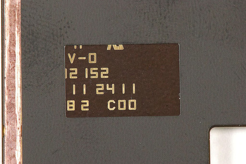
\n\tSome of the markings on the Apple iPad 2’s main system board are obscured by a black sticker that covers most of the board’s underside.
\n
\n\tPhoto by: Bill Detwiler / TechRepublic
\n\tCaption by: Bill Detwiler
\n\tBefore we can see the chips on the Apple iPad 2’s main PCB, we’ll need to remove the EMI shields from the top of the board.
\n
\n\tPhoto by: Bill Detwiler / TechRepublic
\n\tCaption by: Bill Detwiler
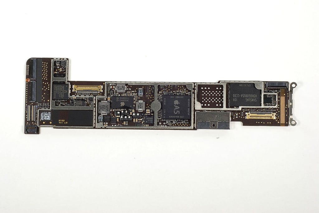
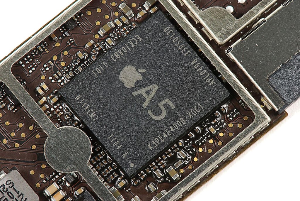
\n\tWith the EMI shields removed, we can see the chips mounted to Apple iPad 2’s main PCB.
\n
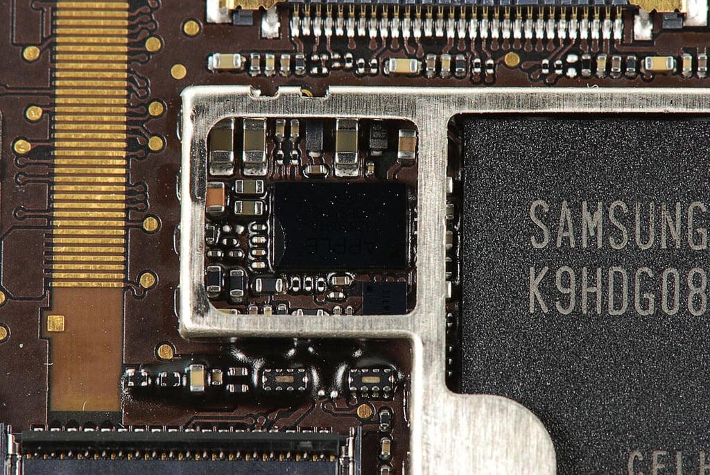
\n\tPhoto by: Bill Detwiler / TechRepublic
\n\tCaption by: Bill Detwiler
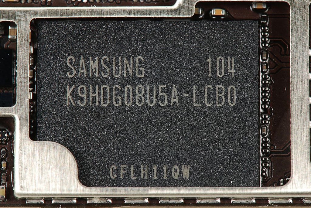
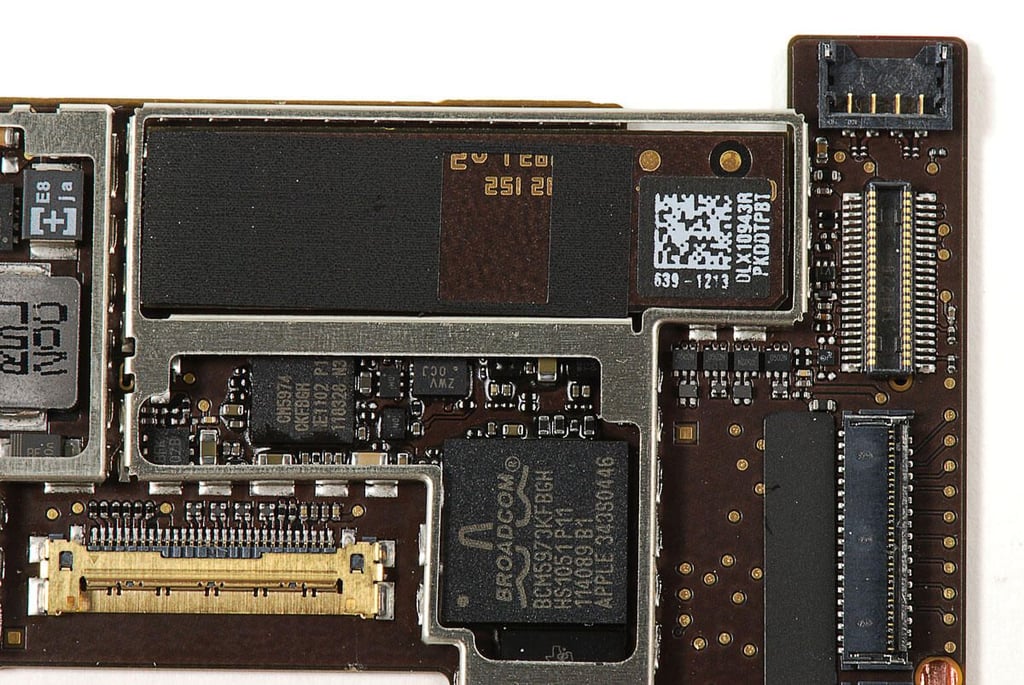
\n\tOur Apple iPad 2 has a 16GB Samsung NAND Flash chip (K9HDG08U5A-LCB0).
\n
\n\tPhoto by: Bill Detwiler / TechRepublic
\n\tCaption by: Bill Detwiler
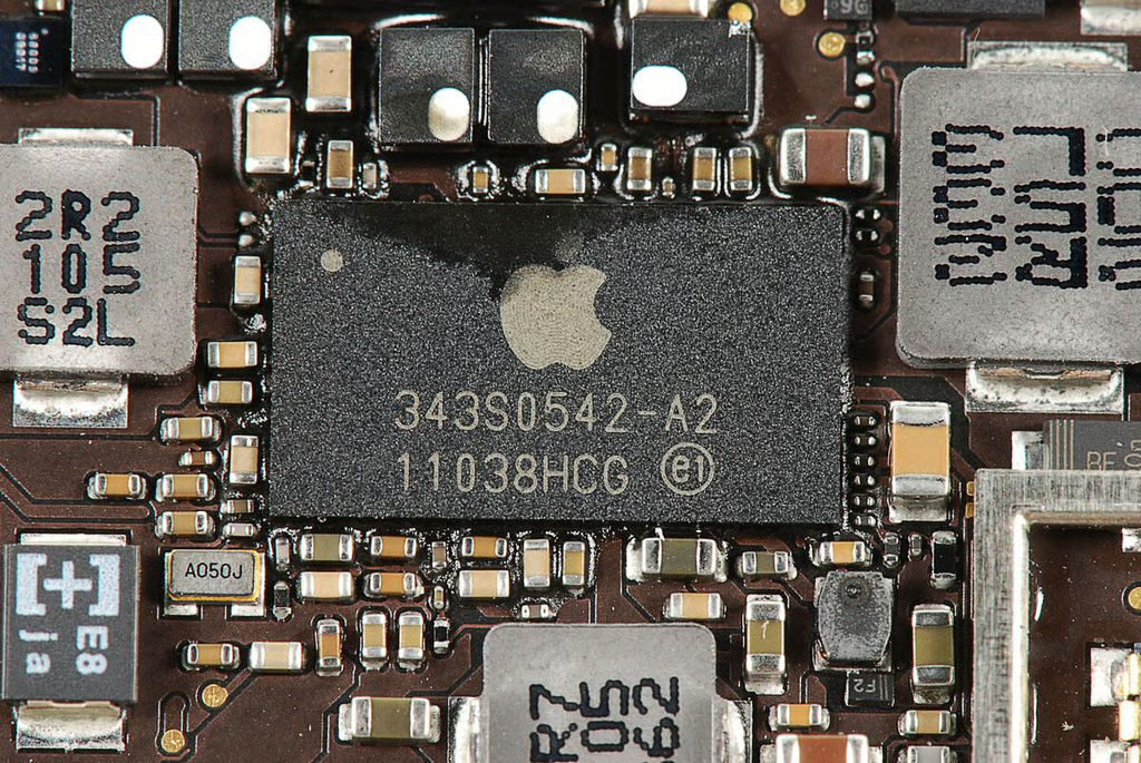
\n\tApple branded chip with markings 343S0542-A2 11038HCG.
\n
\n\tPhoto by: Bill Detwiler / TechRepublic
\n\tCaption by: Bill Detwiler
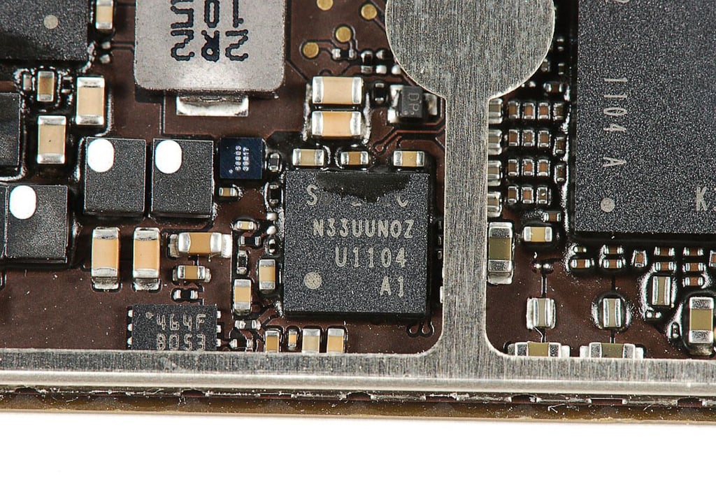
\n\tSome of the markings on thi chip are too faint to read, but these are visible N33UUN0Z U1104 A1.
\n
\n\tPhoto by: Bill Detwiler / TechRepublic
\n\tCaption by: Bill Detwiler
\n\tThis chips has no markings.
\n
\n\tPhoto by: Bill Detwiler / TechRepublic
\n\tCaption by: Bill Detwiler
\n\tPhoto by: Bill Detwiler / TechRepublic
\n\tCaption by: Bill Detwiler
\n\tSome of the markings on this Texas Instruments chip are obscured by the metal bracket for one of the EMI sheilds.
\n
\n\tPhoto by: Bill Detwiler / TechRepublic
\n\tCaption by: Bill Detwiler
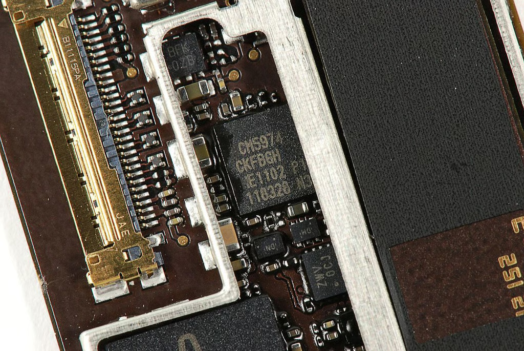
\n\tChip with markings: CM5974 CKFBGH E1102 P! 118328 N3
\n
\n\tPhoto by: Bill Detwiler / TechRepublic
\n\tCaption by: Bill Detwiler
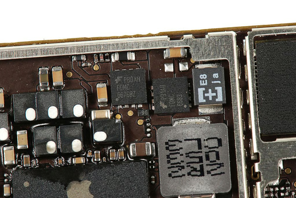
\n\tThe Apple iPad 2 had two chips from Fairchild Semiconductor with the following markings:
\n
\n\tPB0AH
\n\tFDMC
\n\t6676BZ
\n
\n\tPB1AU
\n\tFDMC
\n\t6683
\n
\n\tPhoto by: Bill Detwiler / TechRepublic
\n\tCaption by: Bill Detwiler
\n\tThe Apple iPad 2’s wireless card is mounted to the top of main PCB.
\n
\n\tPhoto by: Bill Detwiler / TechRepublic
\n\tCaption by: Bill Detwiler
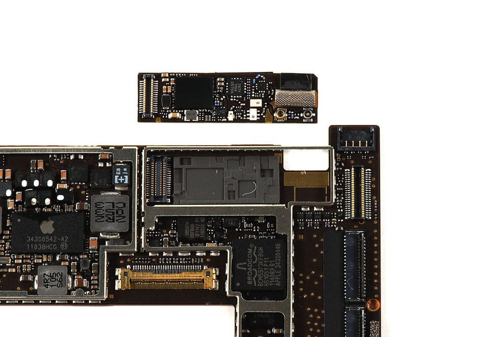
\n\tI removed the wireless card from the Apple iPad 2’s main PCB using a thin metal blade. I’ll be interested to see if the iPad 2 3G version has a different wireless card. I assume it will.
\n
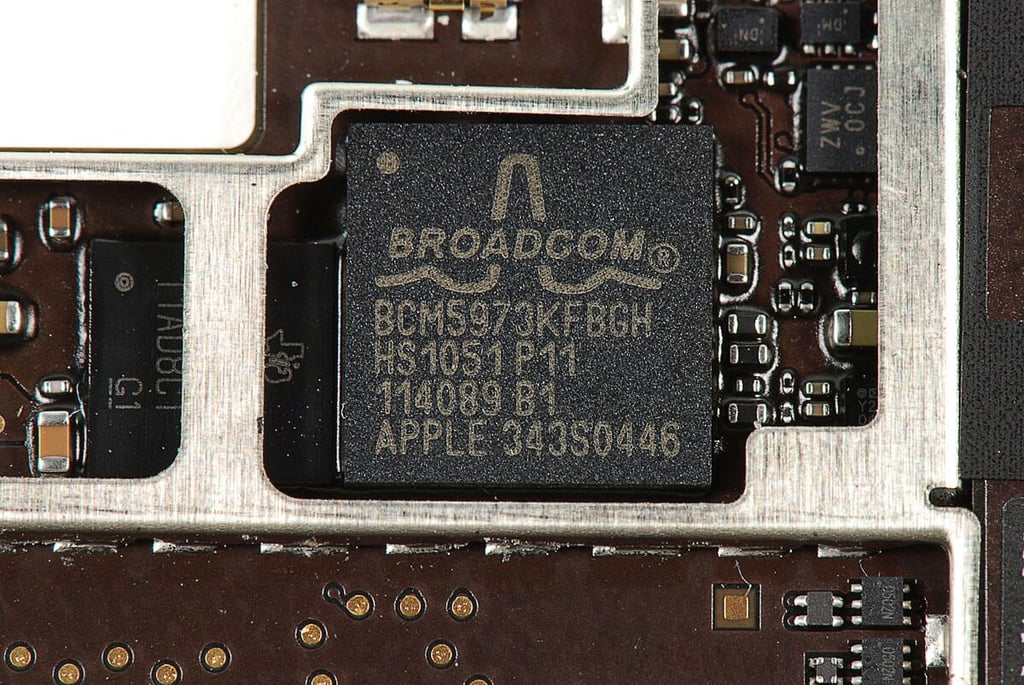
\n\tPhoto by: Bill Detwiler / TechRepublic
\n\tCaption by: Bill Detwiler
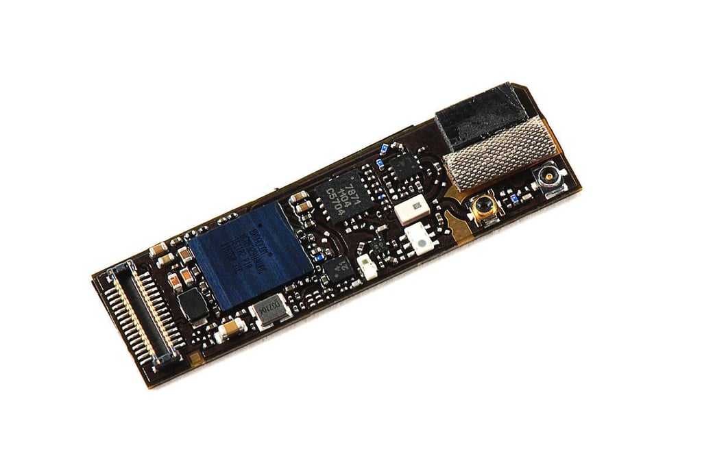
\n\tThe Apple iPad 2’s wireless card has a Broadcom BCM4329 1HKUBC “low-power 802.11n with Bluetooth 2.1 + EDR and FM transceiver” chip.
\n
\n\tPhoto by: Bill Detwiler / TechRepublic
\n\tCaption by: Bill Detwiler
\n\tThe Apple iPad 2 was more difficult to crack open than the original iPad or iPad 3G. Its front panel, battery, main PCB, and many of the ribbon cables inside are glued to the metal frame. In fact, the iPad 2 is constructed more like an iPod Touch than the other tablets I’ve cracked open. Cracking open the Motorola XOOM a snap compared to the iPad 2.
\n
\n\tPhoto by: Bill Detwiler / TechRepublic
\n\tCaption by: Bill Detwiler
Bill Detwiler is the Editor for Technical Content and Ecosystem at Celonis. He is the former Editor in Chief of TechRepublic and previous host of TechRepublic's Dynamic Developer podcast and Cracking Open, CNET and TechRepublic's popular online show. Previously, Bill was an IT manager in the social research and energy industries. He has bachelor's and master's degrees from the University of Louisville, where he has also lectured on computer crime and crime prevention.


