Skip to content

TechRepublic

  • Top Products
  • AI
  • Developer
  • Payroll
  • Security
  • Project Management
  • Accounting
  • CRM
  • Academy
Resources
  • TechRepublic Premium
  • TechRepublic Academy
  • Newsletters
  • Resource Library
  • Forums
  • Sponsored
Go Premium
Popular Topics
  • Top Products
  • AI
  • Developer
  • Payroll
  • Security
  • Project Management
  • Accounting
  • CRM
  • Academy
  • Project Management
  • Innovation
  • Cheat Sheets
  • Big Data
  • Tech Jobs
View All Topics
Go Premium
Hardware

Photos: Bringing nature’s complexity to electronics

By Nick Heath January 12, 2015, 9:19 AM PST

Image
1
of 8

3d-structure-4.jpg
3d-structure-4.jpg
Photos: Bringing nature’s complexity to electronics

Pop-up structures

Image: University of Illinois

Pop-up structures

US researchers have developed a technique for generating 3D circuits that could underpin new medical implants, solar cells and other electronics.

The team at the University of Illinois at Urbana-Champaign devised a process for transforming 2D micro- and nano-structures into 3D, using concepts they described as similar to those used to create children’s 3D pop-up books.

Image: University of Illinois
3d-structure-1.png
3d-structure-1.png
Photos: Bringing nature’s complexity to electronics

Microscopic creations

Image: University of Illinois

Microscopic creations

The process could allow complex 3D structures to be built using materials only a few microns thick. Because the process can be used to create silicon structures, it could be used to help make circuitry for range of electronic devices – from battery anodes, to solar cells, and biomedical devices. Researchers hope the structures will have a use in microelectromechanical components, photonics and optoelectronics and metamaterials.

Image: University of Illinois
3d-structure-5.png
3d-structure-5.png
Photos: Bringing nature’s complexity to electronics

Many materials

Image: University of Illinois

Many materials

The team at Illinois claim this method bypasses some of the constraints on existing methods for building 3D structures at this scale, which limits the classes of materials that can be used and the complexity of the geometries that can be built.

u201cConventional 3D printing technologies are fantastic, but none offers the ability to build microstructures that embed high performance semiconductors, such as silicon,u201d said John Rogers, a Swanlund Chair and professor of materials science and engineering at Illinois.

u201cWe have presented a remarkably simple route to 3D that starts with planar precursor structures formed in nearly any type of material, including the most advanced ones used in photonics and electronics.u201d

Image: University of Illinois
3d-structure-2.png
3d-structure-2.png
Photos: Bringing nature’s complexity to electronics

Compressive buckling

Image: University of Illinois

Compressive buckling

The technique, called compressive buckling, works by printing a 2D structure onto a layer of material that has been compressed. The 2D printed structure is bound to the compressed substrate at several points and when the substrate is released and expands back into its original shape, the 2D structure sat on top rises up into a 3D form.

Image: University of Illinois
3d-structure-10.png
3d-structure-10.png
Photos: Bringing nature’s complexity to electronics

Possible uses

Image: University of Illinois

Possible uses

Because the technique could be combined with other fabrication methods, such as photolithography, and processing techniques used in the semiconductor and photonics industries it could be used to create 3D electronic, optoelectronic and electromagnetic equipment.

Image: University of Illinois
3d-structure-7.png
3d-structure-7.png
Photos: Bringing nature’s complexity to electronics

An array of shapes

Image: University of Illinois

An array of shapes

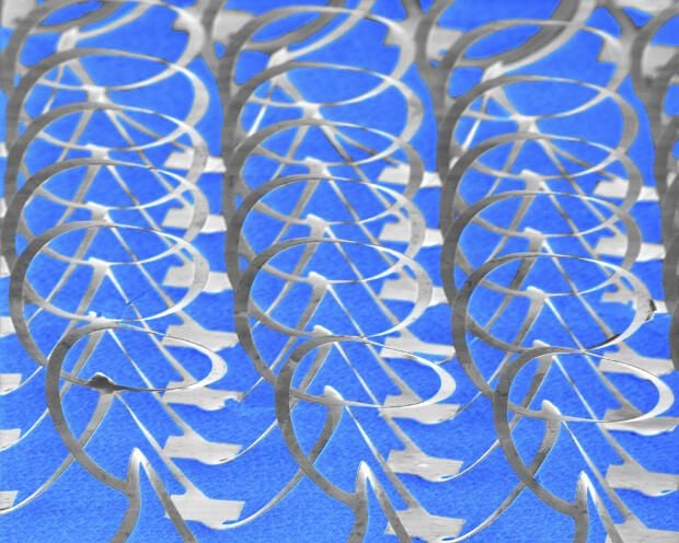
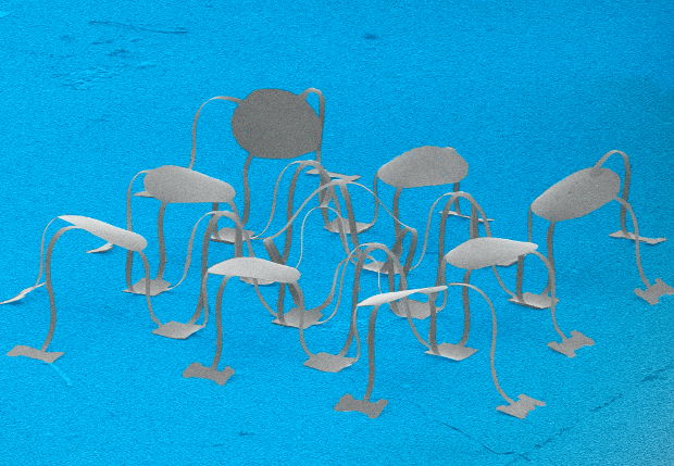
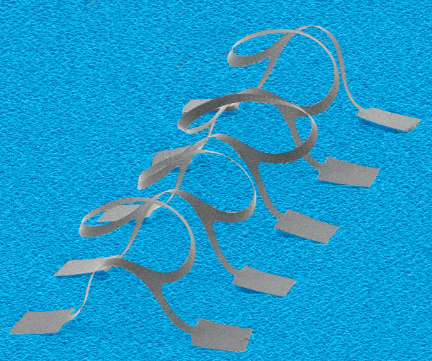
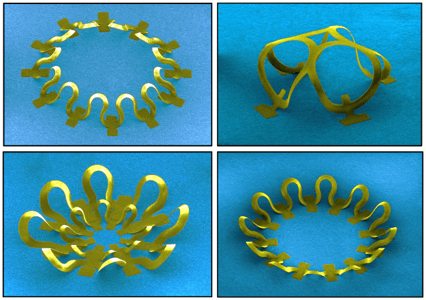
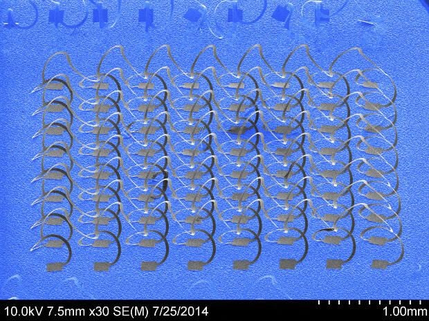
Initial experiments have created more than 40 distinct shapes, ranging from single and multiple helices, toroids and conical spirals, to structures that resemble spherical baskets, cuboid cages, starbursts, flowers, scaffolds and fences.

u201dWe’re now exploiting these ideas in the construction of high performance electronic scaffolds for actively guiding and monitoring growth of tissue cultures, and networks for 3D electronic systems that can bend and shape themselves to the organs of the human body. We’re very enthusiastic about the possibilities,u201d Rogers said.

Image: University of Illinois
3d-structure-3.png
3d-structure-3.png
Photos: Bringing nature’s complexity to electronics

Complex creations

Image: University of Illinois

Complex creations

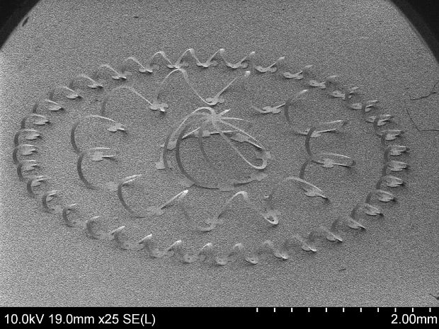
An example of the complexity of the 3D structures that can be created.

Image: University of Illinois
3d-structure-6.jpg
3d-structure-6.jpg
Photos: Bringing nature’s complexity to electronics

Fine detail

Image: University of Illinois

Fine detail

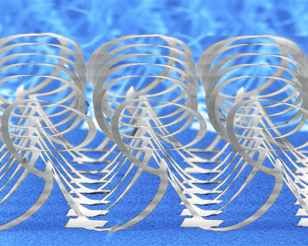
Here you can see the fine detail that can be replicated throughout a structure.

Image: University of Illinois
  • Hardware
  • Account Information

    Share with Your Friends

    Photos: Bringing nature’s complexity to electronics

    Your email has been sent

Share: Photos: Bringing nature's complexity to electronics
Image of Nick Heath
By Nick Heath
Nick Heath is a computer science student and was formerly a journalist at TechRepublic and ZDNet.
  • Account Information

    Contact Nick Heath

    Your message has been sent

  • |
  • See all of Nick's content

Daily Tech Insider

If you can only read one tech story a day, this is it.

TechRepublic TechRepublic
  • TechRepublic on Facebook
  • TechRepublic on X
  • TechRepublic on LinkedIn
  • TechRepublic on YouTube
  • TechRepublic on Pinterest
  • TechRepublic RSS
Services
  • About Us
  • Newsletters
  • RSS Feeds
  • Site Map
  • Site Help & Feedback
  • FAQ
  • Advertise
  • Do Not Sell My Information
  • Careers
Explore
  • Downloads
  • TechRepublic Forums
  • Meet the Team
  • TechRepublic Academy
  • TechRepublic Premium
  • Resource Library
  • Photos
  • Videos
  • Editorial Policy
  • Legal Terms
  • Privacy Policy
© 2025 TechnologyAdvice. All rights reserved.
CLOSE

Create a TechRepublic Account

Get the web's best business technology news, tutorials, reviews, trends, and analysis—in your inbox. Let's start with the basics.

Already registered? Sign In
Use Facebook
Use Linkedin

* - indicates required fields

CLOSE

Sign in to TechRepublic

Not a member? Create an account
Use Facebook
Use Linkedin

Lost your password? Request a new password

CLOSE

Reset Password

Please enter your email adress. You will receive an email message with instructions on how to reset your password.

Check your email for a password reset link. If you didn't receive an email don't forgot to check your spam folder, otherwise contact support.

Back to login
1 Finish Profile
2 Newsletter Preferences
CLOSE

Welcome. Tell us a little bit about you.

This will help us provide you with customized content.

No thanks, continue without
1 Finish Profile
2 Newsletter Preferences
CLOSE

Want to receive more TechRepublic news?

Newsletter Name
Subscribe
Daily Tech Insider
Daily Tech Insider AU
TechRepublic UK
TechRepublic News and Special Offers
TechRepublic News and Special Offers International
Executive Briefing
Innovation Insider
Project Management Insider
Microsoft Weekly
Cloud Insider
Data Insider
Developer Insider
TechRepublic Premium
Apple Weekly
Cybersecurity Insider
Google Weekly
Toggle All
No thanks, continue without

You're All Set

Thanks for signing up! Keep an eye out for a confirmation email from our team. To ensure any newsletters you subscribed to hit your inbox, make sure to add [email protected] to your contacts list.

Back to Home Page
×