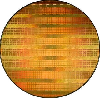
A 300-millimeter wafer containing test SRAM chips made on the 45-nanometer process. The manufacturing technique will be used in mass manufacturing late next year. The test chips typically come out just under two years before mass manufacturing.
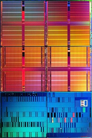
A 45-nanometer test chip. It can hold 153 megabits of memory. The top third consists of memory cells. The middle section contains circuits for input, output and other functions. Those transistors are made so that Intel can test how different transistors come out on the new process. The bottom part is a tester.
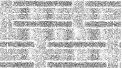
A close-up of a memory cell made using the 45-nanometer process. Those horizontal lines are transistor gates.
Bill Detwiler is the Editor for Technical Content and Ecosystem at Celonis. He is the former Editor in Chief of TechRepublic and previous host of TechRepublic's Dynamic Developer podcast and Cracking Open, CNET and TechRepublic's popular online show. Previously, Bill was an IT manager in the social research and energy industries. He has bachelor's and master's degrees from the University of Louisville, where he has also lectured on computer crime and crime prevention.


