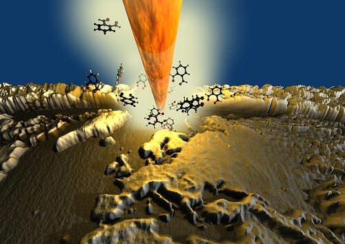
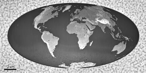
IBM researchers have produced a breakthrough technique that allows scientists to create nanoscale objects. The first mission was to produce the smallest 3D map of the world ever. Using a heated nanoscale silicon tip researchers carved a 22-by-11 micrometer 3D model of the world. At this size, 1000 world maps could fit on a grain of salt. One thousand meters of altitude correspond to roughly eight nanometers (nm).
For more on this story, read Larry Dignan’s blog.
Credit: Advanced Materials
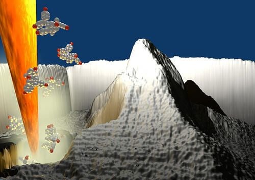
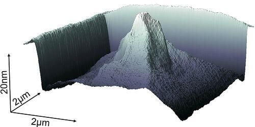
Using this technique, Researchers created a 25-nanometer high replica of the 4,478-meter tall Swiss peak Matterhorn.
Credit: IBM Research – Zurich
IBM describes the nanoscale tip:
“?The micrograph shows a close-up of the nanoscale silicon tip. This tip, borrowed from atomic force microscopy, measures 500 nanometers in length and only a few nanometers at its apex. It is attached to a cantilever that controllably scans the surface of the substrate material with the accuracy of one nanometer \u2013 a millionth of a millimeter. By applying heat and force, the nano-sized tip can remove substrate material based on predefined patterns—operating like a \u201cnanomilling\u201d machine with ultra-high precision.”
Credit: IBM Research – Zurich
Nanoscale tip.
Credit: IBM Research – Zurich
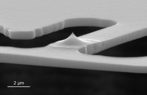
Nanoscale tip.
Credit: IBM Research – Zurich
Nanoscale tip.
Credit: IBM Research – Zurich
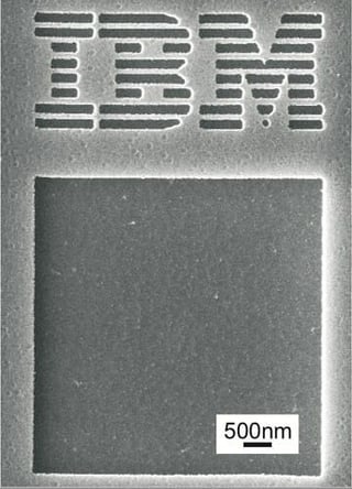
Here’s a nanoscale pattern in silicon.
Credit: Science/AAAS
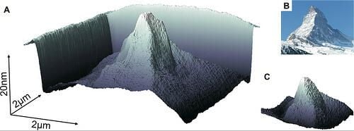
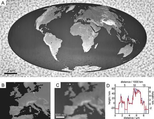
This 25 nanometer replica of the Matterhorn is based on scale of 1:5 billion. Scientists used a nanoscale tip that is 1 million times smaller than an ant to create 2D and 3D patterns and structures as small as 15 nanometers at greatly reduced cost and complexity.
Credit: Science/AAAS
Credit: Science/AAAS
The nano-world was \u201cwritten\u201d \u2013 on a polymer.
Credit: Advanced Materials
The map is composed of 500,000 pixels, each measuring 20 nm2 and was created in only 2 minutes and 23 seconds.
Credit: Advanced Materials
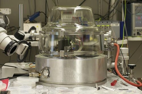
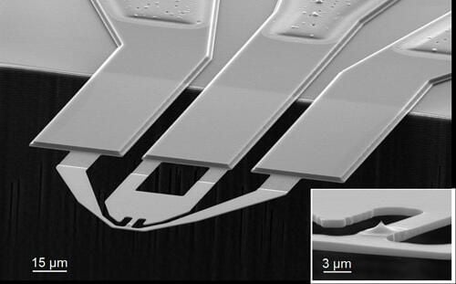
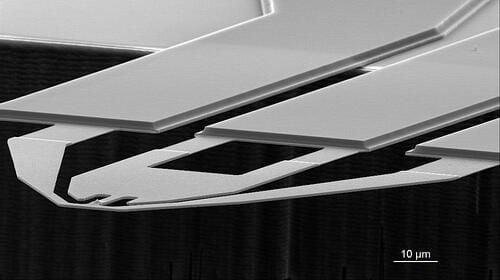
This is the nanopatterning tool used at IBM Research – Zurich. IBM describes it:
Compared to existing nanostructuring techniques, such as e-beam lithography, the compact and low footprint IBM tool promises improved and extended capabilities at very small feature sizes, but at five to ten times less cost and far less complexity.
Credit: Michael Lowry, IBM Research – Zurich
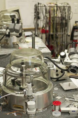
Nanopatterning tool
Credit: Michael Lowry, IBM Research – Zurich
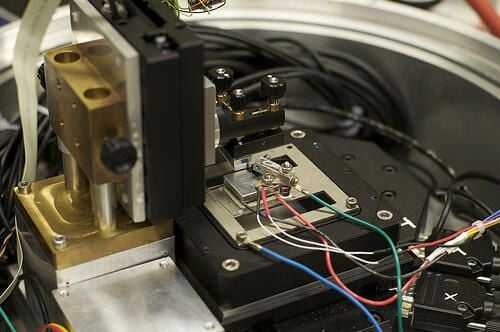
Here’s a closer look at the core micro-electro-mechanical system of the nanopatterning tool.
Credit: Michael Lowry, IBM Research – Zurich
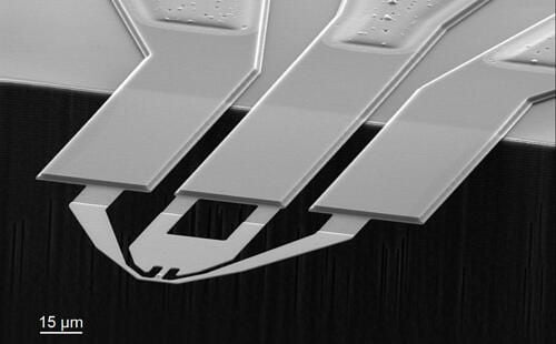
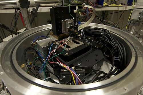
Another look at the nanopatterning tool.
Credit: Michael Lowry, IBM Research – Zurich
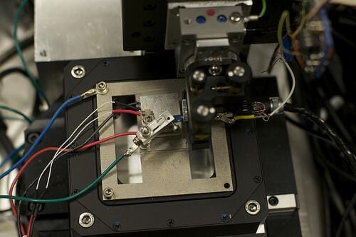
A close-up of the core micro-electro-mechanical system of the tool, which controls the tip.
Credit: Michael Lowry, IBM Research – Zurich
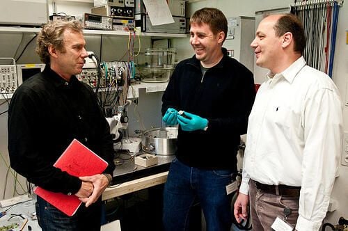
From left to right are the IBM scientists, Dr. Urs Duerig, Dr. Armin Knoll and Dr. Michel Despont, who led this project.
Credit: Michael Lowry, IBM Research – Zurich


