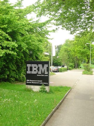
The IBM Research laboratory in Zurich, Switzerland, founded 50 years ago, was Big Blue’s first research facility outside the U.S. It was 25 years ago that the lab made its most famous research breakthrough: the scanning tunneling microscope, which provided the foundation for understanding and working with nanoscale technology.\r\n
\r\nThat breakthrough brought a Nobel Prize in physics in 1986 for Gerd Binnig and Heinrich Rohrer. Only a year later, the lab hit the research jackpot again, when Georg Bednorz and Alex Mueller scooped the same prize for their work on high-temperature superconductivity.\r\n
\r\nTwo Nobels in two years is some achievement, especially considering that IBM Research as a whole has won only three in total.\r\n
\r\nDespite its pedigree, IBM Zurich is quite small. There are 240 employees, and 50 predoctoral and 30 postdoctoral students. IBM Research has 3,500 employees in eight laboratories around the world–with three of those labs in the U.S., including the largest, Thomas J. Watson Research Center.\r\n
\r\nThe work of the lab in Zurich varies widely, from advanced silicon research to helping IBM’s consulting arm win new business.\r\n
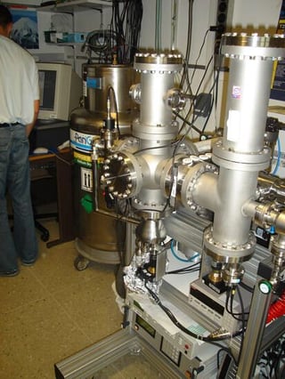
Investigating nanoscale objects is a hugely tricky process–even with a scanning electron microscope–and the research needs to be conducted in a special atmosphere. This particular work, conducted by Walter Riess, the research manager for nanoscale structures and devices, is looking at ways of growing nanowires.\r\n
\r\nA nanowire is an extremely narrow object that has an aspect ratio (the ratio between length and width) of 1,000-to-1 or greater. At this time, nanowires and their possible uses exist only in the realms of research, but Riess and his team are investigating different elements for their suitability for “growing” nanowires, and trying to deduce the properties those wires will have. The aim is to use nanowires to manufacture microprocessors.\r\n
\r\nA microprocessor built from nanowires would, in theory, be much more powerful than current processors since computers are based on electrical signals running through very narrow channels. Today’s microprocessors are so small inside that signals leak and create interference, a problem that will only get bigger as the channels get smaller. Can nanowires conduct electrical signals in nanoscale structures? A lot of science needs to be done before we know the answer to that one.
Another major focus for IBM Zurich is research into ways of dissipating heat from microprocessors.\r\n
\r\nHeat has been an issue in computing since the days of mainframes, when methods like water cooling were used to try to keep processors from melting. It remains a problem today, even though manufacturers have tried a range of possible solutions from complex fans and air cooling to massive heat sinks.\r\n
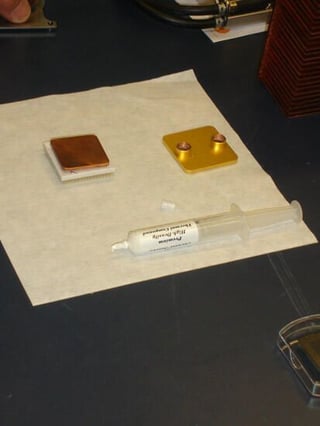
\r\nBruno Michel, the manager for advanced thermal packaging, and his team are working on a procedure that uses a combination of techniques to find more effective cooling. The secret is all in the packaging–Michel’s team is working on a chip package that puts a thermal paste directly on the processor and then attaches a heat sink that can dissipate some of the heat.\r\n
\r\nThis picture shows a chip (at left) with thermal paste added and a copper heat dissipater attached. The liquid cooling attachment (at right) is also experimental.\r\n
\r\nMichel and his team are testing different pastes that can be used as adhesives for attaching processors and have great heat dissipation properties.
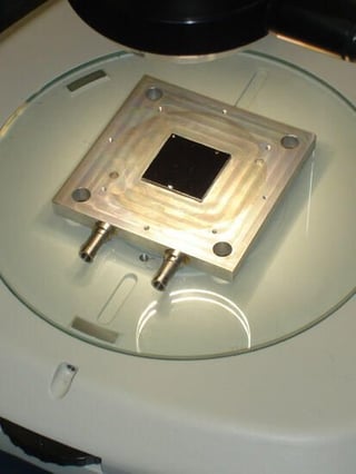
Instead of a heat sink, chips could be covered with a liquid cooling device. This is an “immersion jet impingement” with distributed coolant returns.\r\n
\r\nThe device is about the size of the packaging on a current Pentium processor, but inside that small space there are 50,000 coolant nozzles. The result is that coolant can be circulated very quickly.
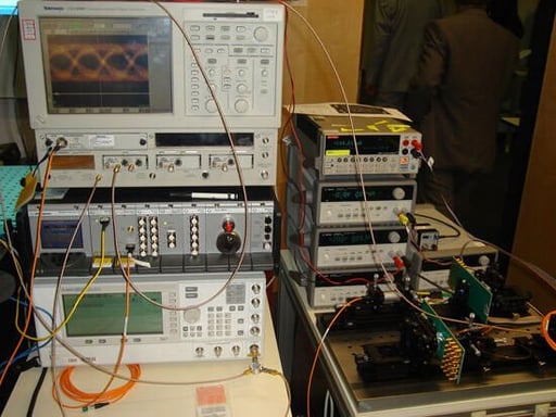
Another area under examination is the input-output bottleneck. As Christian Menolfi, who specializes in I/O links explained, you can see the issue simply by looking at the back of an I/O processor. \r\n
\r\n”Pin counts are getting very large,” Menolfi said. “We are looking at needing 1,000 just for I/O. The complications of the I/O pins are growing faster than the number of pins. This is the package bottleneck.”\r\n
\r\nThe answer, according to Menolfi, is advanced, multichannel signaling (shown in the top-left display). By arranging the I/O channels in the optimum configuration, the Zurich researchers hope to guarantee maximum data throughput.
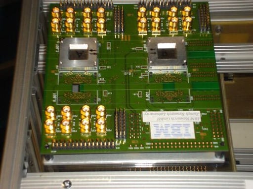
Optical technology could also be used to improve signaling performance. Christoph Berger, a Zurich specialist in this area, demonstrated the theories and practice of optical devices.\r\n
\r\nThis is a four-way, optical interconnect unit. Mountings for two processors are shown, with space for two more.\r\n
\r\nThe processors sit on the mounts. If you attach a microprocessor to a mounting and optical cables to both the input and an output, it’s possible to look down one cable and see through the other.
The more practical side of advanced scientific research can also be seen at the Zurich center, where a range of leading-edge products were on display.\r\n
\r\nThis included projects for ID cards that use the most complex engraving technology, so that a picture is not on a card, but part of the card’s physical structure; a health-monitoring system that uses a cell phone to keep a doctor aware of a patient’s essential health data and will sound an alarm if the parameters change; and a security system that can track people at room level–for situations where it may be OK for someone to walk into the room but not into a particular part of it. \r\n
\r\nOne practical system undergoing final testing with an unnamed transportation company will track containers anywhere in the world and can raise a flag if the container is opened, even if it’s 2,000 miles away. This particular project uses wireless, RFID and related technologies for monitoring and tracking.\r\n
\r\nThe challenge for Zurich scientists has been not so much how to track containers, but how to produce a tracking system that can monitor 10,000 containers individually. Monitors and sensors will have to be powered off batteries for a year or two, keep in contact with a base anything up to 2,000 miles away and still come in at a reasonable cost.
Bill Detwiler is the Editor for Technical Content and Ecosystem at Celonis. He is the former Editor in Chief of TechRepublic and previous host of TechRepublic's Dynamic Developer podcast and Cracking Open, CNET and TechRepublic's popular online show. Previously, Bill was an IT manager in the social research and energy industries. He has bachelor's and master's degrees from the University of Louisville, where he has also lectured on computer crime and crime prevention.


